

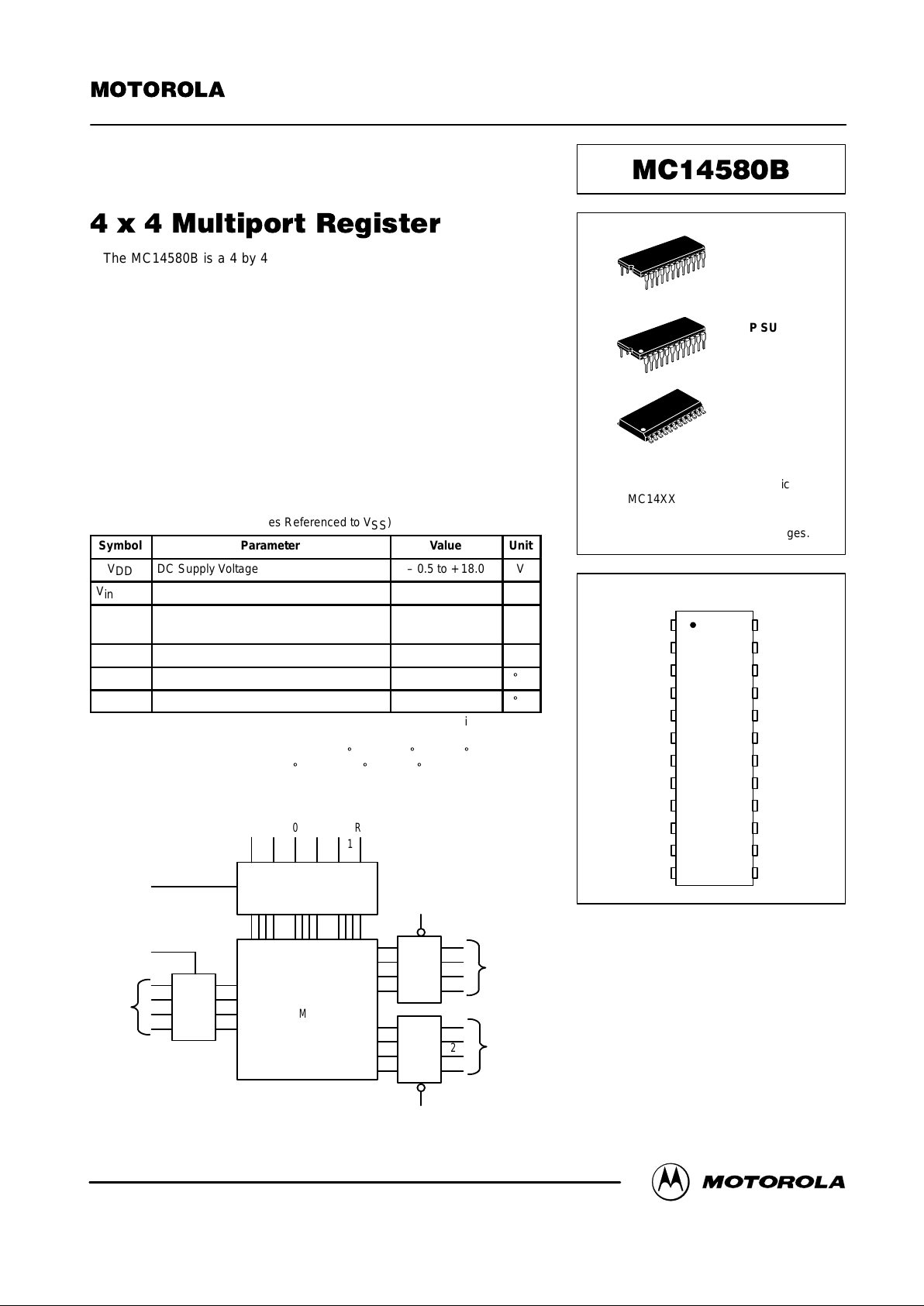
Motorola MC14580BDW, MC14580BCL, MC14580BCP Datasheet
MOTOROLA CMOS LOGIC DATA
1
MC14580B
The MC14580B is a 4 by 4 multiport register useful in small scratch pad
memories, arithmetic operations when coupled with an adder, and other data
storage applications. It allows independent reading of any two words (or the
same word at both outputs) while writing into any one of four words.
Address changing and data entry occur on the rising edge of the clock.
When t he write enable input is low, the contents of any word may b e
accessed but not altered.
• No Restrictions on Clock Input Rise or Fall Times
• 3–State Outputs
• Single Phase Clocking
• Supply Voltage Range = 3.0 Vdc to 18 Vdc
• Capable of Driving Two Low–power TTL Loads or one Low–power
Schottky TTL Load Over the Rated Temperature Range
• Pin Compatible with CD40108
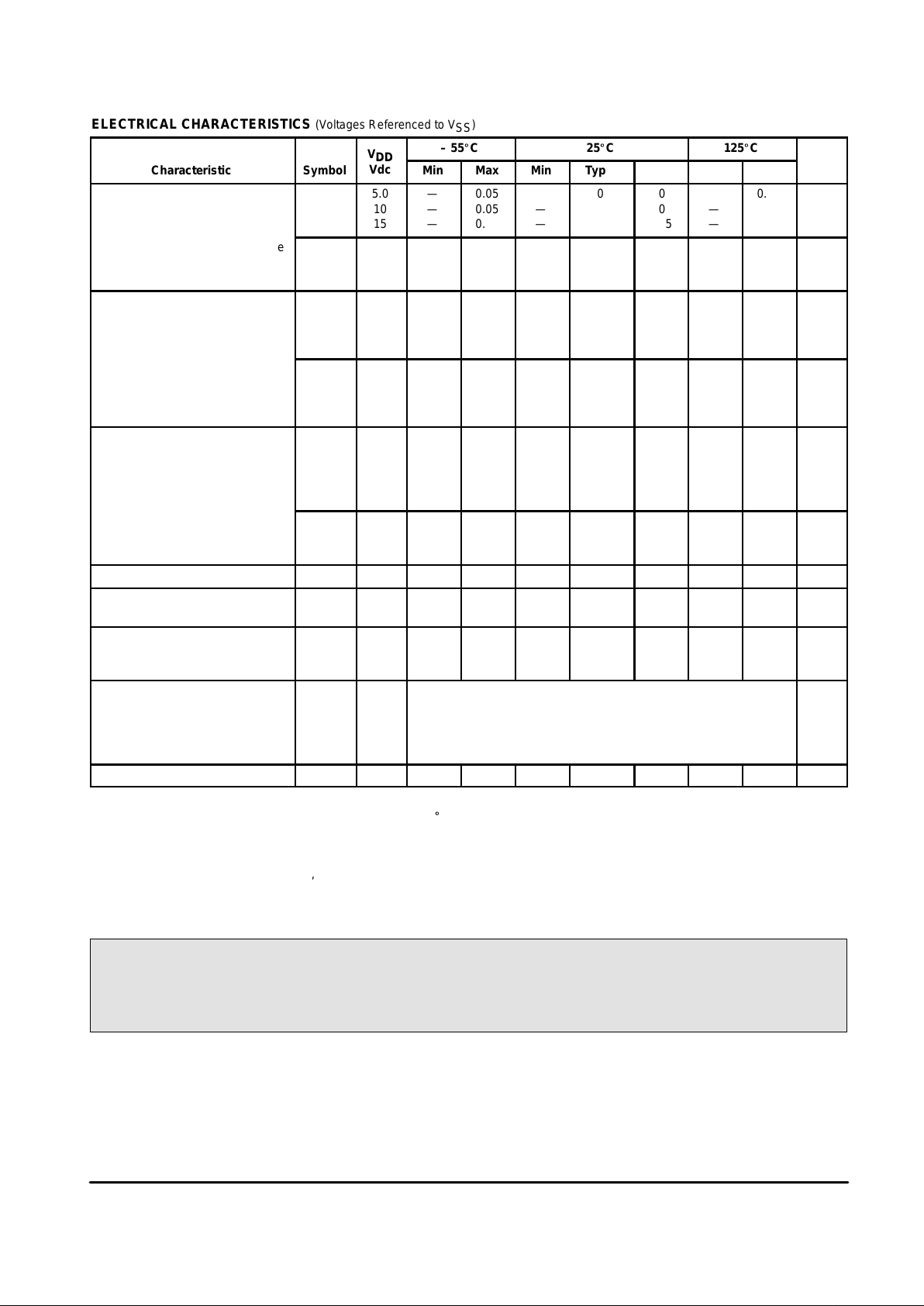
MAXIMUM RATINGS* (Voltages Referenced to V
SS
)
Symbol
Parameter Value Unit
V
DD
DC Supply Voltage – 0.5 to + 18.0 V
Vin, V
out
Input or Output Voltage (DC or Transient) – 0.5 to VDD + 0.5 V
Iin, I
out
Input or Output Current (DC or Transient),
per Pin
± 10 mA
P
D
Power Dissipation, per Package† 500 mW
T
stg
Storage Temperature – 65 to + 150
_
C
T
L
Lead Temperature (8–Second Soldering) 260
_
C
*Maximum Ratings are those values beyond which damage to the device may occur.
†Temperature Derating:
Plastic “P and D/DW” Packages: – 7.0 mW/_C From 65_C To 125_C
Ceramic “L” Packages: – 12 mW/_C From 100_C To 125_C
BLOCK DIAGRAM
CLOCK
16
15
20
191719
18
DATA
INPUT
WE
R1
B
R0
B
R1
AR0A
W1W0
1011141398
DECODER
3–STATE A
3
4
5
6
7
22
23
2
1
21
3–STATE B
4 X 4
MEMORY
VDD = PIN 24
VSS = PIN 12
D0
D1
D2
D3
Q0
A
Q1
A
Q2
A
Q3
A
Q0
B
Q1
B
Q2
B
Q3
B
WORD A
OUTPUT
WORD B
OUTPUT
SEMICONDUCTOR TECHNICAL DATA
Motorola, Inc. 1995
REV 3
1/94
L SUFFIX
CERAMIC
CASE 623
ORDERING INFORMATION
MC14XXXBCP Plastic
MC14XXXBCL Ceramic
MC14XXXBDW SOIC
TA = – 55° to 125°C for all packages.
P SUFFIX
PLASTIC
CASE 709
DW SUFFIX
SOIC
CASE 751E
PIN ASSIGNMENT
Q2
A
Q0
A
3–STATE A
Q2
B
Q3
B
WRITE 0
Q3
A
Q1
A
D0
3–STATE B
Q0
B
Q1
B
V
DD
WE
CLOCK
D3
5
4
3
2
1
10
9
8
7
6
14
15
16
17
18
19
20
13
11
12
21
22
23
24
READ 0
A
READ 1
A
D2
D1
READ 0
B
V
SS
READ 1
B
WRITE 1
MOTOROLA CMOS LOGIC DATAMC14580B
2
ELECTRICAL CHARACTERISTICS (Voltages Referenced to V
SS
)
V
– 55_C 25_C 125_C
Characteristic
Symbol
V
DD
Vdc
Min Max Min Typ # Max Min Max
Unit
Output Voltage “0” Level
Vin = VDD or 0
V
OL
5.0
10
15
—
—
—
0.05
0.05
0.05
—
—
—
0
0
0
0.05
0.05
0.05
—
—
—
0.05
0.05
0.05
Vdc
“1” Level
Vin = 0 or V
DD
V
OH
5.0
10
15
4.95
9.95
14.95
—
—
—
4.95
9.95
14.95
5.0
10
15
—
—
—
4.95
9.95
14.95
—
—
—
Vdc
Input Voltage “0” Level
(VO = 4.5 or 0.5 Vdc)
(VO = 9.0 or 1.0 Vdc)
(VO = 13.5 or 1.5 Vdc)
V
IL
5.0
10
15
—
—
—
1.5
3.0
4.0
—
—
—
2.25
4.50
6.75
1.5
3.0
4.0
—
—
—
1.5
3.0
4.0
Vdc
“1” Level
(VO = 0.5 or 4.5 Vdc)
(VO = 1.0 or 9.0 Vdc)
(VO = 1.5 or 13.5 Vdc)
V
IH
5.0
10
15
3.5
7.0
11
—
—
—
3.5
7.0
11
2.75
5.50
8.25
—
—
—
3.5
7.0
11
—
—
—
Vdc
Output Drive Current
(VOH = 2.5 Vdc) Source
(VOH = 4.6 Vdc)
(VOH = 9.5 Vdc)
(VOH = 13.5 Vdc)
I
OH
5.0
5.0
10
15
– 3.0
– 0.64
– 1.6
– 4.2
—
—
—
—
– 2.4
– 0.51
– 1.3
– 3.4
– 4.2
– 0.88
– 2.25
– 8.8
—
—
—
—
– 1.7
– 0.36
– 0.9
– 2.4
—
—
—
—
mAdc
(VOL = 0.4 Vdc) Sink
(VOL = 0.5 Vdc)
(VOL = 1.5 Vdc)
I
OL
5.0
10
15
0.64
1.6
4.2
—
—
—
0.51
1.3
3.4
0.88
2.25
8.8
—
—
—
0.36
0.9
2.4
—
—
—
mAdc
Input Current I
in
15 — ±0.1 — ±0.00001 ±0.1 — ±1.0 µAdc
Input Capacitance
(Vin = 0)
C
in
— — — — 5.0 7.5 — — pF
Quiescent Current
(Per Package)
I
DD
5.0
10
15
—
—
—
5.0
10
20
—
—
—
0.010
0.020
0.030
5.0
10
20
—
—
—
150
300
600
µAdc
Total Supply Current**†
(Dynamic plus Quiescent,
Per Package)
(CL = 50 pF on all outputs, all
buffers switching)
I
T
5.0
10
15
IT = (1.18 µA/kHz) f + I
DD
IT = (1.91 µA/kHz) f + I
DD
IT = (2.67 µA/kHz) f + I
DD
µAdc
Three–State Leakage Current I
TL
15 — ±0.1 — ±0.0001 ±0.1 — ±3.0 µAdc
#Data labelled “Typ” is not to be used for design purposes but is intended as an indication of the IC’s potential performance.
**The formulas given are for the typical characteristics only at 25_C.
†To calculate total supply current at loads other than 50 pF:
IT(CL) = IT(50 pF) + (CL – 50) Vfk
where: IT is in µA (per package), CL in pF, V = (VDD – VSS) in volts, f in kHz is input frequency, and k = 0.004.
This device contains protection circuitry to guard against damage due to high static voltages or electric fields. However,
precautions must be taken to avoid applications of any voltage higher than maximum rated voltages to this high-impedance
circuit. For proper operation, Vin and V
out
should be constrained to the range VSS ≤ (Vin or V
out
) ≤ VDD.
Unused inputs must always be tied to an appropriate logic voltage level (e.g., either VSS or VDD). Unused outputs must
be left open.
MOTOROLA CMOS LOGIC DATA
3
MC14580B
SWITCHING CHARACTERISTICS* (C
L
= 50 pF, TA = 25_C)
Characteristic
Symbol V
DD
Min Typ # Max Unit
Output Rise and Fall Time
t
TLH
, t
THL
= (1.5 ns/pF) CL + 25 ns
t
TLH
, t
THL
= (0.75 ns/pF) CL + 12.5 ns
t
TLH
, t
THL
= (0.55 ns/pF) CL + 9.5 ns
t
TLH
, t
THL
(Figures 3 and 6)
5.0
10
15
—
—
—
100
50
40
200
100
80
ns
Propagation Delay Time
Clock to Output
t
PLH
, t
PHL
(Figures 3 and 6)
5.0
10
15
—
—
—
650
250
170
1300
500
340
ns
Write Enable Setup Time
(Enabling a Write or Read)
t
su
(Figure 5)
5.0
10
15
800
300
200
400
150
100
—
—
—
ns
Write Enable Removal Time
(Disabling a Write or Read)
t
rem
(Figure 5)
5.0
10
15
0
0
0
– 100
– 50
– 35
—
—
—
ns
Setup Time**
Address, Data to Clock
t
su
(Figure 3)
5.0
10
15
50
30
25
20
0
0
—
—
—
ns
Hold Time**
Clock to Address, Data
t
h
(Figure 3)
5.0
10
15
480
195
150
160
65
50
—
—
—
ns
3–State Enable/Disable Delay Time t
PHZ
, t
PLZ
t
PZH
, t
PZL
(Figures 4 and 7)
5.0
10
15
—
—
—
130
60
45
260
120
90
ns
Clock Pulse Width t
w
(Figure 3)
5.0
10
15
820
330
220
410
165
110
—
—
—
ns
**When loading repetitive highs, the output may glitch low momentarily after the rising edge of Clock. However, data integrity remains unaffected
and data is valid after the propagation delays listed in the Switching Characteristics Table.
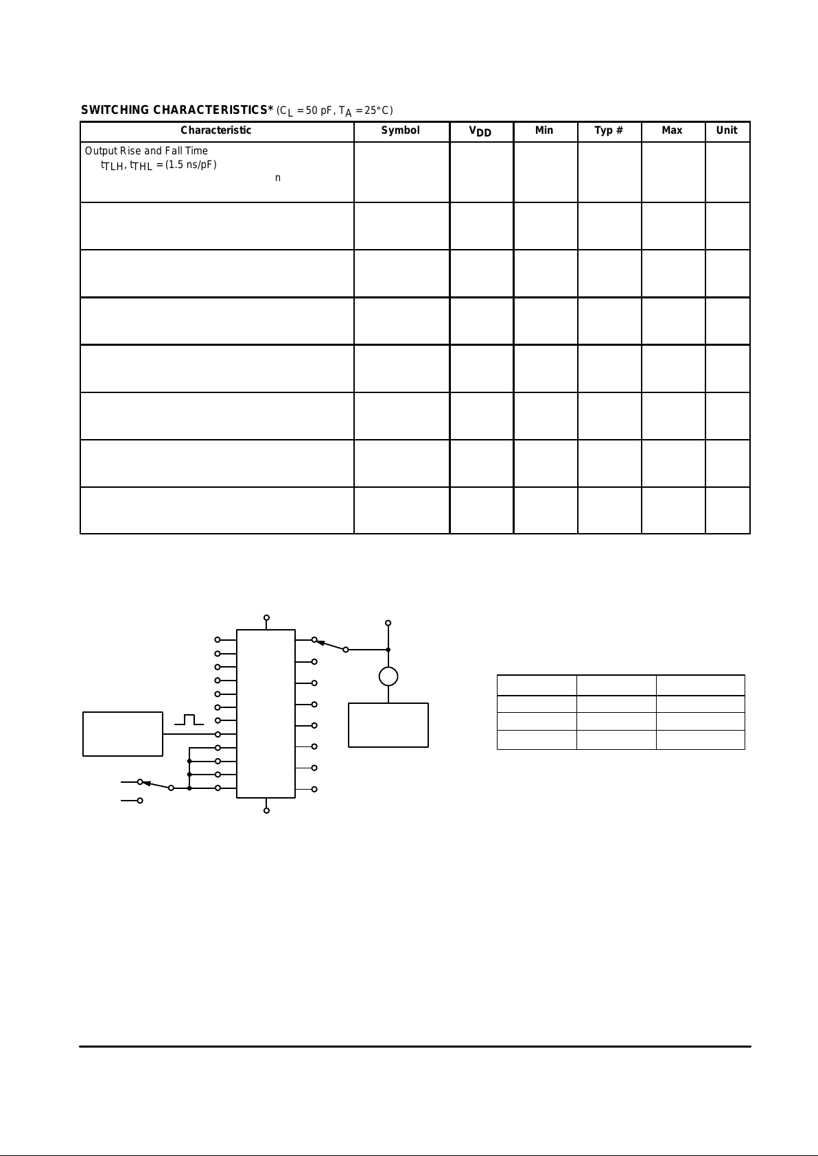
Figure 1. Output Drive Current Test Circuit
Sink Current Source Current
Position of S1 2 1
VGS = V
DD
– V
DD
VDS = V
out
V
out
– V
DD
EXTERNAL
POWER
SUPPLY
V
out
I
DS
V
DD
V
SS
PULSE
GENERATOR
V
DD
V
SS
S1
1
2
WE
W0
W1
R0
A
R1
A
R0
B
R1
B
C
D0
D1
D2
D3
Q0
A
Q1
A
Q2
A
Q3
A
Q0
B
Q1
B
Q2
B
Q3
B
 Loading...