Motorola MC145446AFW Datasheet
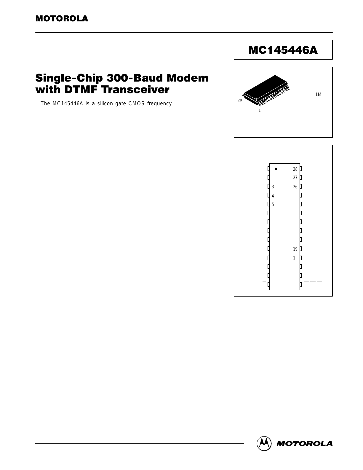
MC145446AMOTOROLA
1
Product Preview
#
%" !$
The MC145446A is a silicon gate CMOS frequency shift keying (FSK)
modem intended for use with telemeter systems or remote control systems over
the telephone network. It replaces the MC145446.
This device is compatible with CCITT V .21 and contains the entire circuit that
provides a full–duplex or half–duplex 300–baud data communication over a pair
of telephone lines. This device also includes the DTMF generator/receiver and
call progress tone detector (CPTD).
The differential line driver has the capability of driving 0 dBm into a 600 Ω load
with a single 5 V power supply. The t ransmit level i s controlled b y the
programmable attenuator in 1 dB steps.
This device also includes a serial control interface and internal control and
status registers that permit a CPU to exercise the following built–in features:
• Single 5 V Power Supply
• Compatible with CCITT V.21
• DTMF Generator and Receiver for All 16 Standard Digits
• Capable of Driving 0 dBm into a 600 Ω Load (VCC = 5 V)
• AGC (Auto Gain Control) Amplifier for DTMF Receiver
• Imprecise Call Progress Tone (400 Hz) Detector
• A Transmit Attenuator Programmable in 1 dB Steps
• 2100 Hz Answer Tone Generator
• Serial Control Interface
• Analog Loopback Configuration for Self Test
• Power–Down Mode, Less than 1 µA
This document contains information on a new product. Specifications and information herein are subject to change without notice.
Order this document
by MC145446A/D
SEMICONDUCTOR TECHNICAL DATA
FW SUFFIX
SOP
CASE 751M
28
1
5
4
3
2
1
10
9
8
7
6
11
12
13
14
20
21
22
23
24
25
26
19
27
28
18
17
16
15
FTLC2
CDA
V
ref
GND
V
CC
TLA
FTLC3
DTMF IN
R/W
V
CC
GND
AGC OUT
X1
X2
TxA1
RxA
RxGC
RxBO
FTLC1
RxD
TxD
DATA I/O
SD
/CD/DV
E
DSI
TxA2
SCK
V
CC
PIN ASSIGNMENT
ORDERING INFORMATION
MC145446AFW SOP
Motorola, Inc. 1996
REV 1
7/96
MC145446A MOTOROLA
2
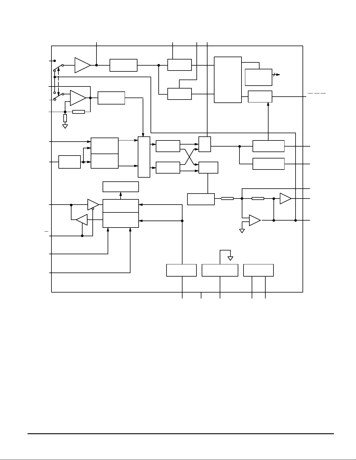
BLOCK DIAGRAM
MUX
CONTROL
SHIFT REGISTER
ANALOG GROUND
GENERATOR
+
+
_
SMOOTHING
FILTER
MUX
FSK
DEMODULATOR
FSK
MODULATOR
DTMF
GENERATOR
MODE CONTROL
LOGIC
STATUS
SHIFT REGISTER
POWER–ON
RESET
CLOCK
GENERATOR
NOISE
FILTER
LOW–BAND
BPF
HIGH–BAND
BPF
MUX/
MIXING
X1 X2V
ref
V
CC
GND
RxBO
DTMF
IN
RxGC
TxD
TLA
DATA
I/O
RxD
SD
/CD/DV
CDA
DSI
TxA1
TxA2
–
LOW–BAND
BPF
FREQUENCY
DETECTER
HIGH–BAND
BPF
CODE
CONVERTER
(DECODER)
TIMING
CIRCUIT
STATUS
REGISTER
SCK
RxA
E
R/W
4
AGC OUT FLTC2 FLTC3
FSK/DTMF LOOPBACK PATH
NOISE
FILTER
65 k
30 k
FLTC1
AGC
CARRIER/CPT
DETECTOR
– 1
LEVEL
CONTROL
MC145446AMOTOROLA
3
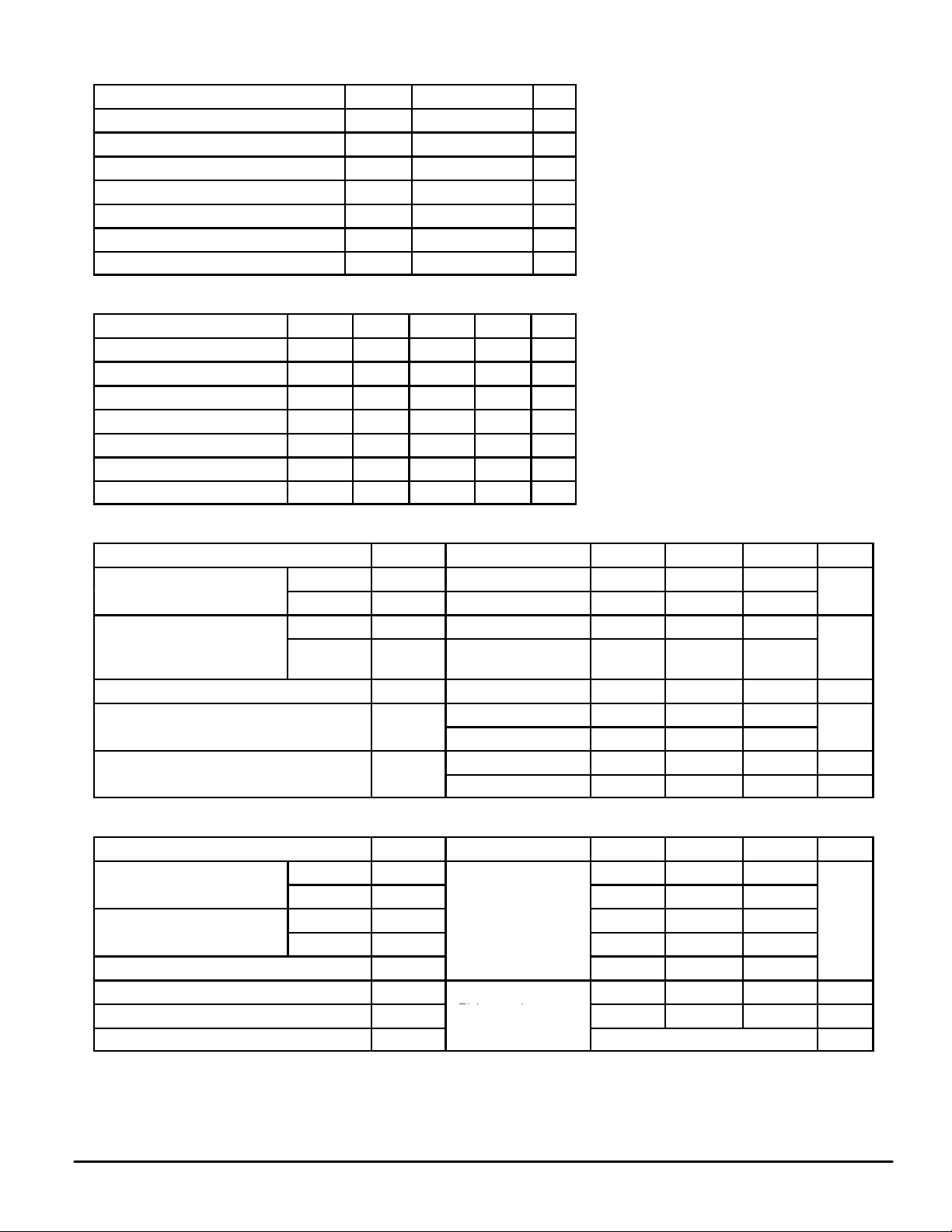
ABSOLUTE MAXIMUM RATINGS (Voltages referenced to V
SS
)
Rating
Symbol Value Unit
DC Supply Voltage V
CC
– 0.5 to 7.0 V
DC Input Voltage V
in
– 0.5 to VCC + 0.5 V
DC Output Voltage V
out
– 0.5 to VCC + 0.5 V
Clamp Diode Current per Pin IIK, I
OK
± 20 mA
DC Current per Pin I
out
± 25 mA
Power Dissipation P
D
500 mW
Storage Temperature Range T
stg
– 65 to 150 °C
RECOMMENDED OPERATING CONDITIONS
Parameter Symbol Min Typ Max Unit
DC Supply Voltage V
CC
4.5 5 5.5 V
DC Input Voltage V
in
0 — V
CC
V
DC Output Voltage V
out
0 — V
CC
V
Input Rise Time t
r
0 — 500 ns
Input Fall Time t
f
0 — 500 ns
Crystal Frequency f
osc
— 3.579545 — MHz
Operating Temperature Range T
A
–20 25 70 °C
DC ELECTRICAL CHARACTERISTICS (V
CC
= 5.0 V ± 10%, TA = – 20 to 70°C)
Characteristic
Symbol Conditions Min Typ Max Unit
H Level V
IH
3.15 — — V
L Level V
IL
— — 1.1
H Level V
OH
IOH = 20 µA VCC – 0.1 VCC – 0.01 — V
L Level V
OL
IOL = 20 µA
IOL = 2 mA
—
—
0.01
—
0.1
0.4
Input Current TxD, E, SCK, DATA I/O, R/W I
in
Vin = VCC or GND — ± 1.0 ± 10.0 µA
I
CC
FSK Mode — 8 —
DCMF Receive Mode — 10 —
I
CC
Power–Down Mode 1 — — 500 µA
Power–Down Supply Current
Power–Down Mode 2 — — 1 µA
TRANSMIT CARRIER CHARACTERISTICS (V
CC
= 5.0 V ± 10%, TA = – 20 to 70°C)
Characteristic
Symbol Conditions Min Typ Max Unit
Mark ‘‘1’’ f
1M
974 980 986 Hz
Space ‘‘0’’ f
1S
3.579545 MHz
1174 1180 1186
Mark ‘‘1’’ f
2M
1644 1650 1656
Space ‘‘0’’ f
2S
1844 1850 1856
Answer Tone f
ans
2090 2100 2110
Transmit Carrier Level VO*
— 7 — dBm
Second Harmonic Energy V2h*
R
TLA
= ∞, RL = 1.2 kΩ,
V
– V
— – 46 — dBm
Out–of–Band Energy VOE*
V
TxA1
– V
TxA2
Figure 2 dBm
*V
TxA1
– V
TxA2
, RL = 1.2 kΩ
This device contains circuitry to protect the
inputs against damage due to high static voltages or electric fields; however, it is advised that
normal precautions be taken to avoid applications of any voltage higher than the maximum
rated voltages to this high impedance circuit.
For proper operation it is recommended that
Vin and V
out
be constrained to the range VSS ≤
(Vin or V
out
) ≤ VDD. Reliability of operation is
enhanced if unused inputs are tied to an
appropriate logic voltage level (e.g., either V
SS
or VDD).
Input Voltage
Output Voltage
Quiescent Supply Current
Carrier Frequency Channel 1
Carrier Frequency Channel 2
Crystal Frequency
Attenuator = 0 dB
mA
MC145446A MOTOROLA
4
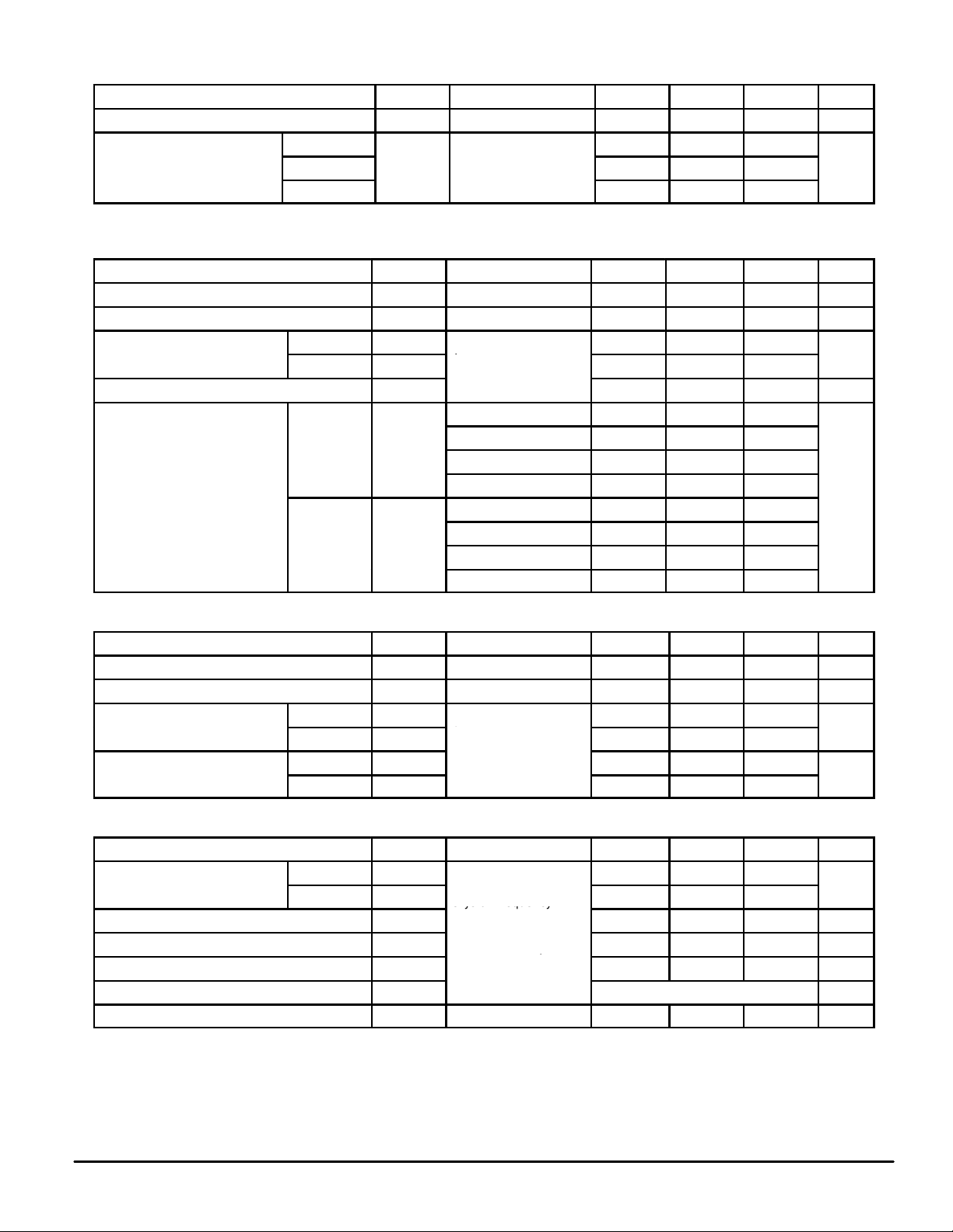
TRANSMIT ATTENUATOR CHARACTERISTICS (V
CC
= 5.0 V ± 10%, TA = – 20 to 70°C)
Characteristic
Symbol Conditions Min Typ Max Unit
Attenuator Range A
RNG
0 — 15 dB
1 dB – 5 dB
– 0.5 — 0.5
6 dB – 9 dB – 1 — 1
10 dB – 15 dB – 1.7 — 1
RECEIVER CHARACTERISTICS (INCLUDES HYBRID, DEMODULATOR, AND CARRIER DETECTOR)
(VCC = 5.0 V ± 10%, TA = – 20 to 70°C)
Characteristic
Symbol Conditions Min Typ Max Unit
Input Impedance R
IRX
RxA Pin 50 — — kΩ
Receiver Carrier Amplitude V
IRX
– 48 — – 12 dBm
Carrier Detect Threshold OFF to ON V
CDON
— – 44 — dBm
ON to OFF V
CDOF
fin = 1.0 kHz
— – 47 —
Hysterisis (V
CDON
– V
CDOF
) HYS 2 — — dB
CD1 = 0, CD0 = 0 — 450 — ms
CD1 = 0, CD0 = 1 — 10 —
CD1 = 1, CD0 = 0 — 10 —
CD1 = 1, CD0 = 1 — 70 —
CD1 = 0, CD0 = 0 — 35 —
CD1 = 0, CD0 = 1 — 35 —
CD1 = 1, CD0 = 0 — 20 —
CD1 = 1, CD0 = 1 — 15 —
CPTD CHARACTERISTICS (V
CC
= 5.0 V ± 10%, TA = – 20 to 70°C)
Characteristic
Symbol Conditions Min Typ Max Unit
Bandpass Filter Center Frequency f
c
— 400 — Hz
Bandpass Filter – 3 dB Band Width ∆
BW
— 140 — Hz
OFF to ON V
TDON
— – 44 — dBm
ON to OFF V
TDOF
fin = 400 Hz
— – 47 —
OFF to ON T
TDON
— 10 — ms
ON to OFF T
TDOF
— 25 —
DTMF TRANSMIT CHARACTERISTICS (V
CC
= 5.0 V ± 10%, TA = – 20 to 70°C)
Characteristic
Symbol Conditions Min Typ Max Unit
Low Group V
fl
— 2.5 — dBm
High Group V
fh
RTLA = ∞
Crystal Frequency
— 3.5 —
High Group Pre–Emphasis P
E
Crystal Frequency
3.579545 MHz
0 — 3 dB
DTMF Distortion DIST
Single Tone Mode
V
– V
,
— 5 — %
DTMF Frequency Variation ∆f
V
V
TxA1
– V
TxA2
,
RL = 1.2 kΩ
– 1 — 1 %
Out–of–Band Energy V
OE
Figure 1 dB
Setup Time t
osc
— 4 — ms
Attenuator Accuracy
A
ACC
Carrier Detect Timing OFF to ON T
ON to OFF T
CDON
CDOFF
CDA = 1.2 5V
dB
Tone Detect Level
Tone Detect Timing
Tone Output Level
CDA = 1.25 V
Attenuator = 0 dB
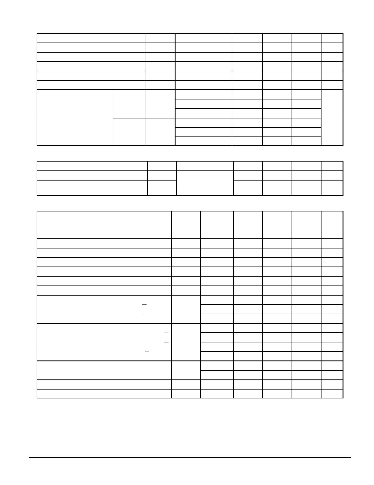
MC145446AMOTOROLA
5
DTMF RECEIVER CHARACTERISTICS (V
CC
= 5.0 V ± 10%, TA = – 20 to 70°C)
Characteristic
Symbol Conditions Min Typ Max Unit
Input Impedance 50 — — kΩ
Detect Signal Level (Each Tone) – 48 — 0 dBm
Twist (High Group Tone/Low Group Tone – 10 — 10 dB
Frequency Detect Band Width (Figure 4) ±1.5% ±2Hz — — —
Frequency No–Detect Band Width (Figure 4) — — ± 3.5 %
CD1 = 0, CD0 = 1 — 25 —
CD1 = 1, CD0 = 0 — 30 —
CD1 = 1, CD0 = 1 — 40 —
CD1 = 0, CD0 = 1 — 25 —
CD1 = 1, CD0 = 0 — 35 —
CD1 = 1, CD0 = 1 — 25 —
DEMODULATOR CHARACTERISTICS (V
CC
= 5.0 V ± 10%, TA = – 20 to 70°C)
Characteristic
Symbol Conditions Min Typ Max Unit
Bit Bias ID
— 5 — %
Bit Error Rate
(CCITT Line Simulation, 511–Bit Pattern)
BER
S/N = 4 dB
— 0.00001 — —
SWITCHING CHARACTERISTICS (V
CC
= 5.0 V ± 10%, TA = – 20 to 70°C)
Characteristic
Symbol
Timing
Diagram
Reference
No.
Min Typ Max Unit
Input Pulse Width (H) E, SCK t
wh
1 50 — — ns
Input Pulse Width (L) E, SCK t
wl
2 50 — — ns
Clock Cycle t
c
3 100 — — ns
Input Rise Time t
r
4 — — 2 µs
Input Fall Time t
f
5 — — 2 µs
Recovery Time E to SCK t
rec
6, 18 50 — — ns
Setup Time DATA to SCK
7 50 — — ns
R/W↓ to DATA 9 100 — — ns
R/W↑ to DATA 12 50 — — ns
Hold Time SCK to DATA
8 50 — — ns
E to R/W 10 50 — — ns
DATA to R/W 14 50 — — ns
R/W to DATA 15 50 — — ns
Read Data Delay Time E to DATA
13 — — 50 ns
SCK to DATA 17 — — 50 ns
Enable Minimum Interval t
we
11 — — 450 ns
Mode Switch Minimum Interval t
wm
16 — — 600 ns
DTMF Detect Timing OFF to ON T
ON to OFF T
CDON
CDOFF
ms
Input Level = – 24 dBm
t
su
t
h
t
d
 Loading...