

Motorola MC145443BP, MC145442BDW, MC145443BDW Datasheet
MOTOROLA
SEMICONDUCTOR TECHNICAL DATA
Order this document
by MC145442B/D
MC145442B
Single-Chip 300-Baud Modem
The MC145442B and MC145443B silicon–gate CMOS single–chip low–
speed modems contain a complete frequency shift keying (FSK) modulator,
demodulator, and filter. These devices are compatible with CCITT V.21
(MC145442B) and Bell 103 (MC145443B) specifications. Both devices provide
full–duplex or half–duplex 300–baud data communication over a pair of
telephone lines. They also include a carrier detect circuit for the demodulator
section and a duplexer circuit for direct operation on a telephone line through a
simple transformer.
• MC145442B Compatible with CCITT V.21
• MC145443B Compatible with Bell 103
• Low–Band and High–Band Band–Pass Filters On–Chip
• Simplex, Half–Duplex, and Full–Duplex Operation
• Originate and Answer Mode
• Analog Loopback Configuration for Self Test
• Hybrid Network Function On–Chip
• Carrier Detect Circuit On–Chip
• Adjustable Transmit Level and CD
• On–Chip Crystal Oscillator (3.579 MHz)
• Single +5 V Power Supply Operation
• Internal Mid–Supply Generator
• Power–Down Mode
• Pin Compatible with MM74HC943
• Capable of Driving –9 dBm into a 600 Ω Load
Delay Timing
MC145443B
P SUFFIX
20
1
20
1
ORDERING INFORMATION
MC145442BP Plastic DIP
MC145443BP Plastic DIP
MC145442BDW SOG Package
MC145443BDW SOG Package
PIN ASSIGNMENT
DSI
1
LB
2
CD
3
CDT
4
RxD 5
V
6
DD
CDA
7
X
8
out
X
9
in
FB
10
PLASTIC DIP
CASE 738
DW SUFFIX
SOG PACKAGE
CASE 751D
20
TLA
19
V
18
Exl
17
TxA
16
RxA1
15
RxA2
14
SQT
13
MODE
12
V
11
TxD
AG
SS
REV 1
9/00
Motorola, Inc. 2000
MC145442B•MC145443BMOTOROLA
1
15
RxA2
16
RxA1
2
LB
13
MODE
14
SQT
11
TxD
20
TLA
8
X
out
X
in
*Refer to the FB pin description.
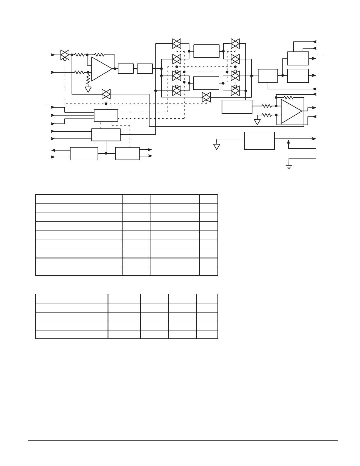
9
OSCILLATOR
–
+
MODULATOR
MODE
CONTROL
AAF S/H
CLOCK
DIVIDER
BLOCK DIAGRAM
LOW–BAND
BPF
HIGH–BAND
BPF
SAMPLING CLOCK: 77.82 kHz
SAMPLING CLOCK: 19.46 kHz
SMOOTHING
FILTER
INTERNAL
V
AG
AC AMP
ANALOG
GROUND
GENERATOR
4
CDT
7
CDA
CARRIER
DETECT
*
DEMOD
–
+
3
CD
5
RxD
10
FB
1
DSI
17
TxA
18
ExI
19
V
AG
6
V
DD
12
V
SS
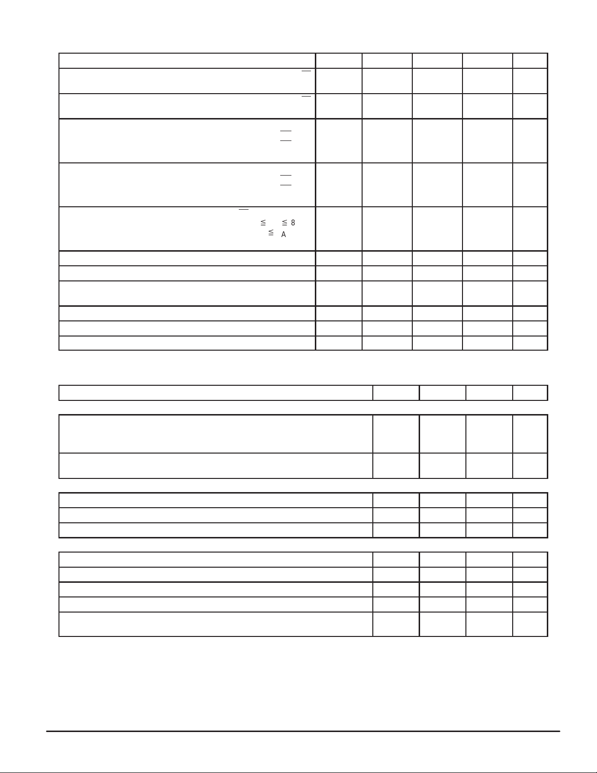
ABSOLUTE MAXIMUM RATINGS (Voltages Referenced to V
Rating Symbol Value Unit
Supply Voltage V
DC Input Voltage V
DC Output Voltage V
Clamp Diode Current, per Pin IIK, I
DC Output Current, per Pin I
Power Dissipation P
Operating Temperature Range T
Storage Temperature Range T
DD
out
out
stg
in
D
A
–0.5 to VDD + 0.5 V
–0.5 to VDD + 0.5 V
OK
)
SS
–0.5 to 7.0 V
±20 mA
±28 mA
500 mW
–40 to 85 °C
–65 to 150 °C
RECOMMENDED OPERATING CONDITIONS
Parameter Symbol Min Max Unit
Supply Voltage V
DC Input or Output Voltage Vin, V
Input Rise or Fall Time tr, t
Crystal Frequency* f
*Changing the crystal frequency from 3.579 MHz will change the output frequencies. The
change in output frequency will be proportional to the change in crystal frequency .
DD
out
f
crystal
4.5 5.5 V
0 V
— 500 ns
3.2 5.0 MHz
DD
V
This device contains circuitry to protect the
inputs against damage due to high static voltages or electric fields; however, it is advised that
normal precautions be taken to avoid application
of any voltage higher than maximum rated
voltages to this high impedance circuit. For
proper operation it is recommended that Vin and
V
be constrained to the range VSS ≤ (Vin or
out
V
) ≤ VDD).
out
Unused inputs must always be tied to an
appropriate logic voltage level (e.g., either V
or VDD).
SS
MC145442B•MC145443B MOTOROLA
2
DC ELECTRICAL CHARACTERISTICS (V
Characteristic Symbol Min Typ Max Unit
High–Level Input Voltage LB
Low–Level Input Voltage LB
High–Level Output Voltage
IOH = 20 µACD
IOH = 2 mA CD
IOH = 20 µAX
Low–Level Output Voltage
IOL = 20 µACD
IOL = 2 mA CD
IOL = 20 µAX
Input Current LB, TxD, Mode, SQT
Quiesent Supply Current (Xin or f
Power–Down Supply Current — 200 300 µA
Input Capacitance X
VAG Output Voltage (IO = ±10 µA) V
CDA Output Voltage (IO = ±10 µA) V
Line Driver Feedback Resistor R
RxA1, RxA2 (0° x TA x 85°C)
RxA1, RxA2 (–40° x TA < 0°C)
= 3.579 MHz) I
crystal
= 5.0 V ±10%, TA = –40° to 85°C)
DD
Xin, TxD, Mode, SQT
Xin, TxD, Mode, SQT
, RxD
, RxD
out
, RxD
, RxD
out
X
in
All Other Inputs
in
V
V
V
OH
V
OL
I
DD
C
AG
CDA
IH
IL
in
in
VDD – 0.8
3.15
—
—
VDD – 0.1
3.7
—
—
—
—
—
—
—
—
— 7 10 mA
—
—
2.4 2.5 2.6 V
1.1 1.2 1.3 V
f
10 20 30 kΩ
—
—
—
—
—
—
VDD – 0.05
—
—
0.05
—
10
—
—
10
—
—
—
0.8
1.1
—
—
—
0.1
0.4
—
±1.0
±12
±20
±10
—
10
V
V
V
V
µA
pF
AC ELECTRICAL CHARACTERISTICS
(VDD = 5.0 V ±10%, TA = –40° to 85°C, Crystal Frequency = 3.579 MHz ±0.1%; See Figure 1)
Characteristic
TRANSMITTER
Power Output on TxA
RL = 1.2 kΩ, R
RL = 1.2 kΩ, R
Second Harmonic Power
RL = 1.2 kΩ
RECEIVE FILTER AND HYBRID
Hybrid Input Impedance RxA1, RxA2 40 50 — kΩ
FB Output Impedance — 16 — kΩ
Adjacent Channel Rejection –48 — — dBm
DEMODULATOR
Receive Carrier Amplitude –48 — –12 dBm
Dynamic Range — 36 — dB
Bit Jitter (S/N = 30 dB, Input = –38 dBm, Bit Rate = 300 baud) — 100 — µs
Bit Bias — 5 — %
Carrier Detect Threshold On to Off
(CDA = 1.2 V or CDA grounded through a 0.1 µF capacitor) Off to On
TLA
TLA
= ∞
= 5.5 kΩ
Min Typ Max Unit
–13
–10
— –56 — dBm
—
—
–12
–9
–44
–47
–11
–8
—
—
dBm
dBm
MC145442B•MC145443BMOTOROLA
3
3.579 MHz ± 0.1%
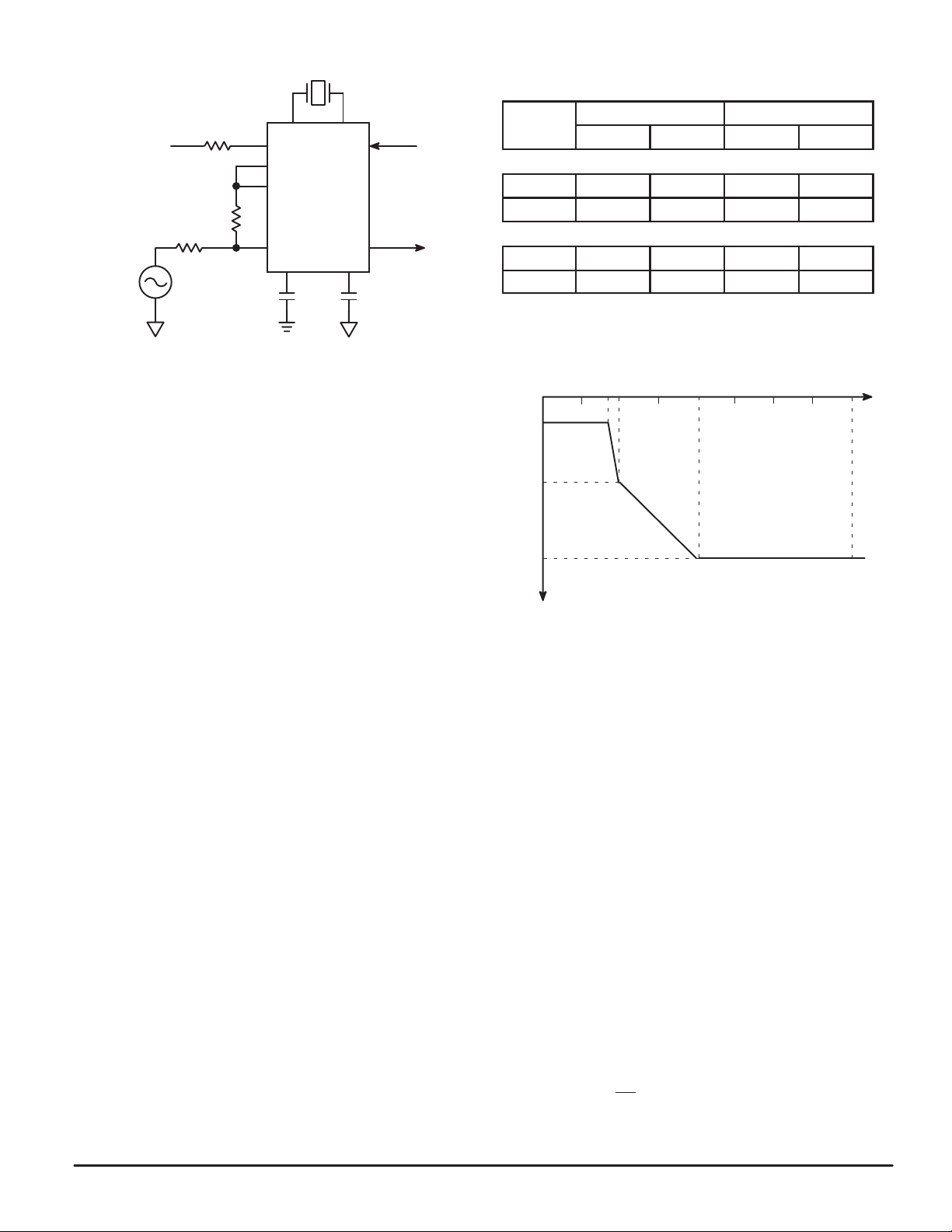
CDT
98
X
in
11
TxD
5
RxD
FB
10
0.1 µF
C
FB
TEST
INPUT
R
TLA
V
DD
600 Ω
600 Ω
TEST
OUTPUT
20
17
15
16
0.1 µF
X
out
TLA
TxA
RxA2
MC145442B
MC145443B
RxA1
CDT
4
C
Figure 1. AC Characteristics Evaluation Circuit
T able 1. Bell 103 and CCITT V.21
Frequency Characteristics
Originate Mode Answer Mode
D
in
D
out
Data
Bell 103 (MC145443B)
Space 1070 Hz 2025 Hz 2025 Hz 1070 Hz
Mark 1270 Hz 2225 Hz 2225 Hz 1270 Hz
CCITT V.21 (MC145442B)
Space 1180 Hz 1850 Hz 1850 Hz 1180 Hz
Mark 980 Hz 1650 Hz 1650 Hz 980 Hz
NOTE: Actual frequencies may be ±5 Hz assuming 3.579545 MHz
RELATIVE TO THE TRANSMIT CARRIER LEVEL INT O 600 Ω (kHz)
Transmit Receive Transmit Receive
crystal is used.
MAXIMUM LEVEL OF OUT–OF–BAND ENERGY
25664163.4 420
PIN DESCRIPTIONS
V
DD
Positive Power Supply (Pin 6)
This pin is normally tied to 5.0 V.
V
SS
Negative Power Supply (Pin 12)
This pin is normally tied to 0 V.
V
AG
Analog Ground (Pin 19)
Analog ground is internally biased to (VDD – VSS)/2. This
pin must be decoupled by a capacitor from VAG to VSS and a
capacitor from VAG to VDD. Analog ground is the common
bias line used in the switched capacitor filters, limiter, and
slicer in the demodulation circuitry .
TLA
Transmit Level Adjust (Pin 20)
This pin is used to adjust the transmit level. Transmit level
adjustment range is typically from –12 dBm to –9 dBm. (See
Applications Information.
TxD
Transmit Data (Pin 11)
Binary information is input to the transmit data pin. Data
entered for transmission is modulated using FSK techniques.
A logic high input level represents a mark and a logic low
represents a space (see Table 1).
TxA
Transmit Carrier (Pin 17)
This is the output of the line driver amplifier. The transmit
carrier is the digitally synthesized sine wave output of the
modulator derived from a crystal oscillator reference. When a
3.579 MHz crystal is used the frequency outputs shown in
Table 1 apply. (See
)
Applications Information
.)
0
–20
–25
15 dB/OCTAVE
–55
TRANSMIT CARRIER LEVEL (dBm)
–60
Figure 2. Out–of–Band Energy
ExI
External Input (Pin 18)
The external input is the non–inverting input to the line
driver. It is provided to combine an auxiliary audio signal or
speech signal to the phone line using the line driver. This pin
should be connected to VAG if not used. The average level
must be the same as VAG to maintain proper operation. (See
Applications Information
.)
DSI
Driver Summing Input (Pin 1)
The driver summing input may be used to connect an external signal, such as a DTMF dialer, to the phone line. A
series resistor, R
AV (see
Applications Information
, is needed to define the voltage gain
DSI
and Figure 6). When applying a signal to the DSI pin, the modulator should be
squelched by bringing SQT (pin 14) to a logic high level. The
voltage gain, AV, is calculated by the formula AV = –Rf/R
(where Rf ≈ 20 kΩ). For example, a 20 kΩ resistor for R
DSI
DSI
will provide unity gain (AV = –20 kΩ/20 kΩ = –1). This pin
must be left open
if not used.
RxD
Receive Data (Pin 6)
The receive data output pin presents the digital binary data
resulting from the demodulation of the receive carrier. If no
carrier is present, CD
high, the receive data output (RxD) is
clamped high.
MC145442B•MC145443B MOTOROLA
4
 Loading...