

Motorola MC14543BCL, MC14543BD, MC14543BCP Datasheet
MOTOROLA CMOS LOGIC DATA
1
MC14543B
!# !
!#
" $ !
The MC14543B BCD–to–seven segment latch/decoder/driver is designed
for use with liquid crystal readouts, and is constructed with complementary
MOS (CMOS) enhancement mode d evices. The circuit provides t he
functions of a 4–bit storage latch and an 8421 BCD–to–seven segment
decoder and driver. The device has the capability to invert the logic levels of
the output combination. The phase (Ph), blanking (BI), and latch disable (LD)
inputs are used to reverse the truth table phase, blank the display , and store
a BCD code, respectively. For liquid crystal (LC) readouts, a square wave is
applied to the Ph input of the circuit and the electrically common backplane
of the d isplay. The o utputs of the circuit are c onnected directly to the
segments of t he LC r eadout. F or o ther t ypes o f readouts, such as
light–emitting diode (LED), incandescent, gas discharge, and fluorescent
readouts, connection diagrams are given on this data sheet.
Applications include instrument (e.g., counter, DVM etc.) display driver,
computer/calculator display driver, cockpit display driver, and various clock,
watch, and timer uses.
• Latch Storage of Code
• Blanking Input
• Readout Blanking on All Illegal Input Combinations
• Direct LED (Common Anode or Cathode) Driving Capability
• Supply Voltage Range = 3.0 V to 18 V
• Capable of Driving Two Low–power TTL Loads, One Low–power
Schottky TTL Load or Two HTL Loads Over the Rated Temperature
Range
• Pin–for–Pin Replacement for CD4056A (with Pin 7 Tied to VSS).
• Chip Complexity: 207 FETs or 52 Equivalent Gates
MAXIMUM RATINGS* (Voltages referenced to V
SS
)
Rating
Symbol Value Unit
DC Supply Voltage V
DD
– 0.5 to + 18 V
Input Voltage, All Inputs V
in
– 0.5 to VDD + 0.5 V
DC Input Current per Pin I
in
± 10 mA
Operating Temperature Range T
A
– 55 to + 125
_
C
Power Dissipation, per Package† P
D
500 mW
Storage Temperature Range T
stg
– 65 to + 150
_
C
Maximum Continuous Output Drive
Current (Source or Sink) per Output
I
OHmax
I
OLmax
10 mA
Maximum Continuous Output Power*
(Source or Sink) per Output
P
OHmax
P
OLmax
70 mW
*P
OHmax
= IOH (VOH – VDD) and P
OLmax
= IOL (VOL – VSS)
*Maximum Ratings are those values beyond which damage to the device may occur.
†Temperature Derating:
Plastic “P and D/DW” Packages: – 7.0 mW/_C From 65_C To 125_C
Ceramic “L” Packages: – 12 mW/_C From 100_C To 125_C
TRUTH TABLE
Inputs Outputs
LD BI Ph* D C B A a b c d e f g Display
X 1 0 X X X X 0 0 0 0 0 0 0 Blank
1 0 0 0 0 0 0 1 1 1 1 1 1 0 0
1 0 0 0 0 0 1 0 1 1 0 0 0 0 1
1 0 0 0 0 1 0 1 1 0 1 1 0 1 2
1 0 0 0 0 1 1 1 1 1 1 0 0 1 3
1 0 0 0 1 0 0 0 1 1 0 0 1 1 4
1 0 0 0 1 0 1 1 0 1 1 0 1 1 5
1 0 0 0 1 1 0 1 0 1 1 1 1 1 6
1 0 0 0 1 1 1 1 1 1 0 0 0 0 7
1 0 0 1 0 0 0 1 1 1 1 1 1 1 8
1 0 0 1 0 0 1 1 1 1 1 0 1 1 9
1 0 0 1 0 1 0 0 0 0 0 0 0 0 Blank
1 0 0 1 0 1 1 0 0 0 0 0 0 0 Blank
1 0 0 1 1 0 0 0 0 0 0 0 0 0 Blank
1 0 0 1 1 0 1 0 0 0 0 0 0 0 Blank
1 0 0 1 1 1 0 0 0 0 0 0 0 0 Blank
1 0 0 1 1 1 1 0 0 0 0 0 0 0 Blank
0 0 0 X X X X ** **
† † † † Inverse of Output Display
Combinations as above
Above
X = Don’t care
† = Above Combinations
* = For liquid crystal readouts, apply a square wave to Ph
For common cathode LED readouts, select Ph = 0
For common anode LED readouts, select Ph = 1
** = Depends upon the BCD code previously applied when
LD = 1
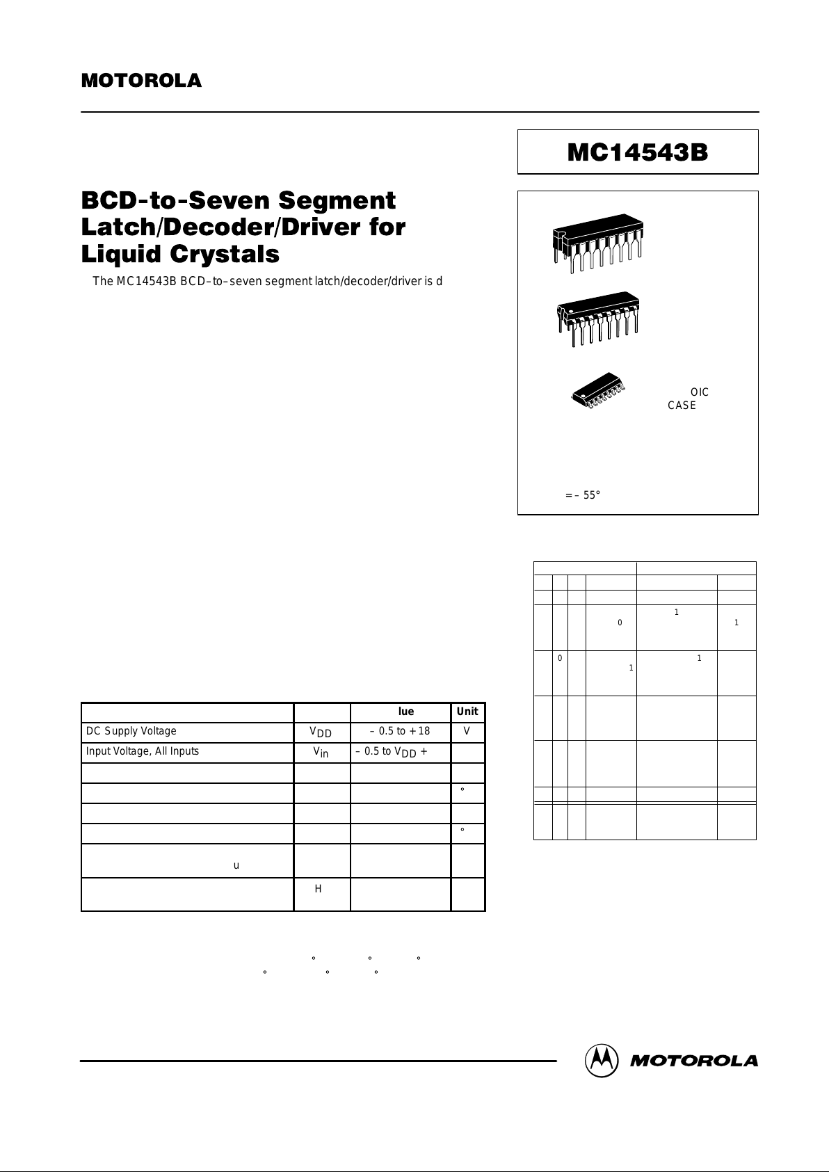
SEMICONDUCTOR TECHNICAL DATA
Motorola, Inc. 1995
REV 3
1/94
L SUFFIX
CERAMIC
CASE 620
ORDERING INFORMATION
MC14XXXBCP Plastic
MC14XXXBCL Ceramic
MC14XXXBD SOIC
TA = – 55° to 125°C for all packages.
P SUFFIX
PLASTIC
CASE 648
D SUFFIX
SOIC
CASE 751B
MOTOROLA CMOS LOGIC DATAMC14543B
2
ELECTRICAL CHARACTERISTICS (Voltages Referenced to V
SS
)
V
DD
– 55_C 25_C 125_C
Characteristic
Symbol
DD
Vdc
Min Max Min Typ # Max Min Max
Unit
Output Voltage “0” Level
Vin = VDD or 0
V
OL
5.0
10
15
—
—
—
0.05
0.05
0.05
—
—
—
0
0
0
0.05
0.05
0.05
—
—
—
0.05
0.05
0.05
Vdc
“1” Level
Vin = 0 or V
DD
V
OH
5.0
10
15
4.95
9.95
14.95
—
—
—
4.95
9.95
14.95
5.0
10
15
—
—
—
4.95
9.95
14.95
—
—
—
Vdc
Input Voltage “0” Level
(VO = 4.5 or 0.5 Vdc)
(VO = 9.0 or 1.0 Vdc)
(VO = 13.5 or 1.5 Vdc)
V
IL
5.0
10
15
—
—
—
1.5
3.0
4.0
—
—
—
2.25
4.50
6.75
1.5
3.0
4.0
—
—
—
1.5
3.0
4.0
Vdc
“1” Level
(VO = 0.5 or 4.5 Vdc)
(VO = 1.0 or 9.0 Vdc)
(VO = 1.5 or 13.5 Vdc)
V
IH
5.0
10
15
3.5
7.0
11
—
—
—
3.5
7.0
11
2.75
5.50
8.25
—
—
—
3.5
7.0
11
—
—
—
Vdc
Output Drive Current
(VOH = 2.5 Vdc) Source
(VOH = 4.6 Vdc)
(VOH = 0.5 Vdc)
(VOH = 9.5 Vdc)
(VOH = 13.5 Vdc)
I
OH
5.0
5.0
10
10
15
– 3.0
– 0.64
—
– 1.6
– 4.2
—
—
—
—
—
– 2.4
– 0.51
—
– 1.3
– 3.4
– 4.2
– 0.88
– 10.1
– 2.25
– 8.8
—
—
—
—
—
– 1.7
– 0.36
—
– 0.9
– 2.4
—
—
—
—
mAdc
(VOL = 0.4 Vdc) Sink
(VOL = 0.5 Vdc)
(VOL = 9.5 Vdc)
(VOL = 1.5 Vdc)
I
OL
5.0
10
10
15
0.64
1.6
—
4.2
—
—
—
—
0.51
1.3
—
3.4
0.88
2.25
10.1
8.8
—
—
—
—
0.36
0.9
—
2.4
—
—
—
mAdc
Input Current I
in
15 — ±0.1 — ±0.00001 ±0.1 — ±1.0 µAdc
Input Capacitance C
in
— — — — 5.0 7.5 — — pF
Quiescent Current
(Per Package) Vin = 0 or VDD,
I
out
= 0 µA
I
DD
5.0
10
15
—
—
—
5.0
10
20
—
—
—
0.005
0.010
0.015
5.0
10
20
—
—
—
150
300
600
µAdc
Total Supply Current**†
(Dynamic plus Quiescent,
Per Package)
(CL = 50 pF on all outputs, all
buffers switching)
I
T
5.0
10
15
IT = (1.6 µA/kHz) f + I
DD
IT = (3.1 µA/kHz) f + I
DD
IT = (4.7 µA/kHz) f + I
DD
µAdc
#Noise immunity specified for worst–case input combination.
Noise Margin for both “1” and “0” level = 1.0 V min @ VDD = 5.0 V
= 2.0 V min @ VDD = 10 V
= 2.5 V min @ VDD = 15 V
†To calculate total supply current at loads other than 50 pF:
IT(CL) = IT(50 pF) + 3.5 x 10⁻³ (CL – 50) VDDf
where: IT is in µA (per package), CL in pF, VDD in V, and f in kHz is input frequency.
**The formulas given are for the typical characteristics only at 25_C.
MOTOROLA CMOS LOGIC DATA
3
MC14543B
SWITCHING CHARACTERISTICS* (C
L
= 50 pF, TA = 25_C)
Characteristic
Symbol V
DD
Min Typ Max Unit
Output Rise Time
t
TLH
= (3.0 ns/pF) CL + 30 ns
t
TLH
= (1.5 ns/pF) CL + 15 ns
t
TLH
= (1.1 ns/pF) CL + 10 ns
t
TLH
5.0
10
15
—
—
—
100
50
40
200
100
80
ns
Output Fall Time
t
THL
= (1.5 ns/pF) CL + 25 ns
t
THL
= (0.75 ns/pF) CL + 12.5 ns
t
THL
= (0.55 ns/pF) CL + 12.5 ns
t
THL
5.0
10
15
—
—
—
100
50
40
200
100
80
ns
Turn–Off Delay Time
t
PLH
= (1.7 ns/pF) CL + 520 ns
t
PLH
= (0.66 ns/pF) CL + 217 ns
t
PLH
= (0.5 ns/pF) CL + 160 ns
t
PLH
5.0
10
15
—
—
—
605
250
185
1210
500
370
ns
Turn–On Delay Time
t
PHL
= (1.7 ns/pF) CL + 420 ns
t
PHL
= (0.66 ns/pF) CL + 172 ns
t
PHL
= (0.5 ns/pF) CL + 130 ns
t
PHL
5.0
10
15
—
—
—
505
205
155
1650
660
495
ns
Setup Time t
su
5.0
10
15
350
450
500
—
—
—
ns
Hold Time t
h
5.0
10
15
40
30
20
—
—
—
ns
Latch Disable Pulse Width (Strobing Data) t
WH
5.0
10
15
250
100
80
125
50
40
—
—
—
ns
*The formulas given are for the typical characteristics only.
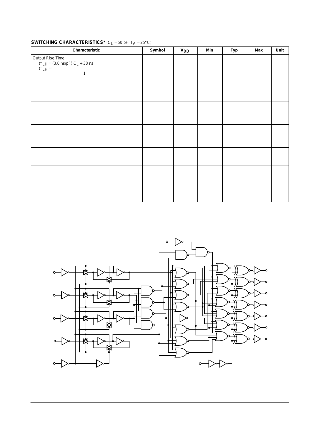
LOGIC DIAGRAM
VDD = PIN 16
VSS = PIN 8
B 3
LD 1
D 4
C 2
A 5
PHASE 6
14 g
15 f
13 e
12 d
11 c
10 b
9 a
BI 7
 Loading...