

Motorola MC145200, MC145201, MC145191, MC145190 Datasheet
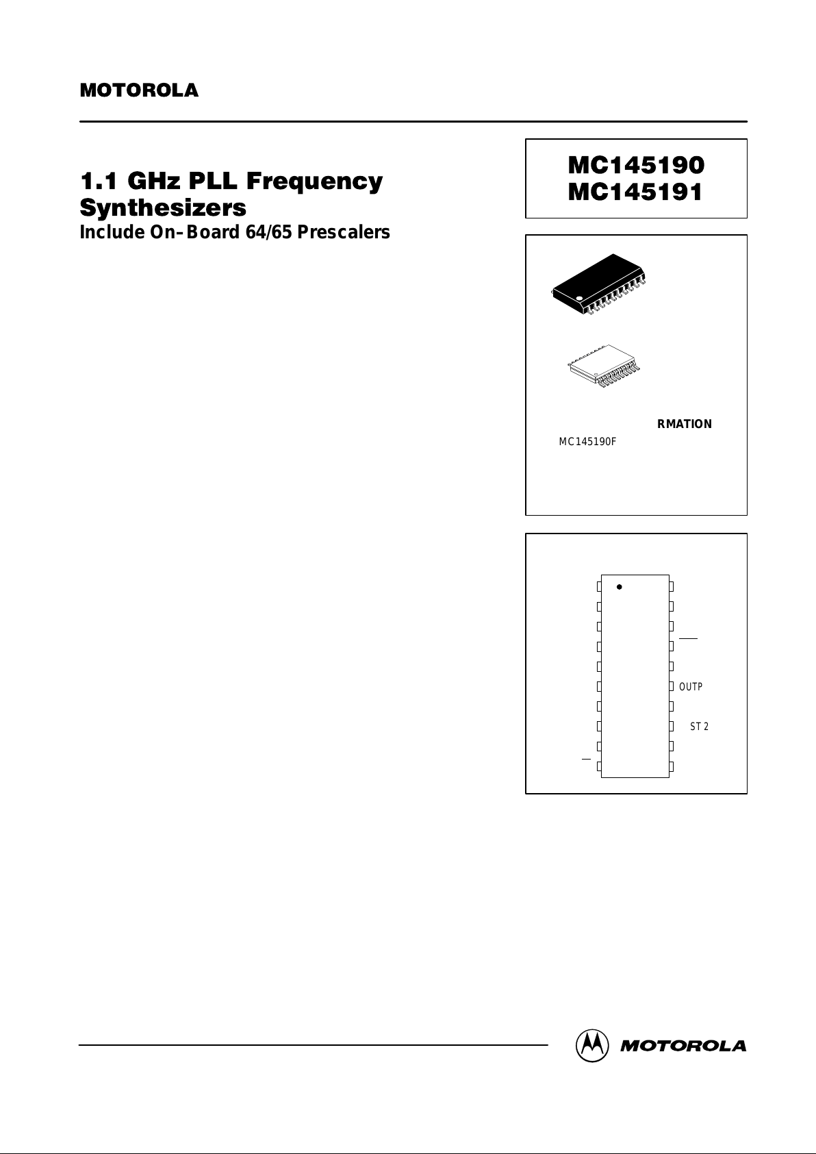
MC145190•MC145191MOTOROLA
1
Include On–Board 64/65 Prescalers
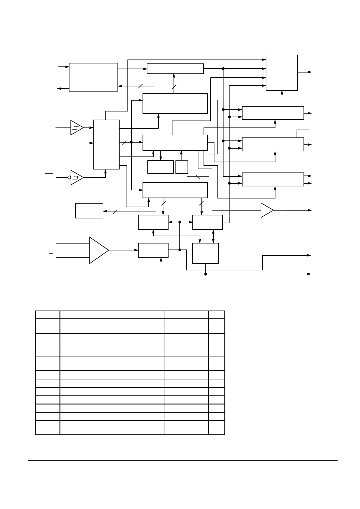
The MC145190 and MC145191 are single–package synthesizers with serial
interfaces capable of direct usage up to 1.1 GHz. A special architecture makes
these PLLs very easy to program because a byte–oriented format is utilized.
Due to the patented BitGrabber
registers, no address/steering bits are
required for
random access
of the three registers. Thus, tuning can be
accomplished via a 3–byte serial transfer to the 24–bit A register. The interface
is both SPI and MICROWIRE
compatible.
Each device features a single–ended current source/sink phase detector
output and a double–ended phase detector output. Both phase detectors have
linear transfer functions (no dead zones). The maximum current of the
single–ended phase detector output is determined by an external resistor tied
from the Rx pin to ground. This current can be varied via the serial port.
The MC145190 features logic–level converters and high–voltage phase/
frequency detectors; the detector supply may range up to 9.5 V. The
MC145191 has lower–voltage phase/frequency detectors optimized for
single–supply systems of 5 V ±10%.
Each part includes a differential RF input which may be operated in a
single–ended mode. Also featured are on–board support of an external crystal
and a programmable reference output. The R, A, and N counters are fully
programmable. The C register (configuration register) allows the parts to be
configured to meet various applications. A patented feature allows the C
register to shut off unused outputs, thereby minimizing system noise and
interference.
In order to have consistent lock times and prevent erroneous data from being
loaded into the counters, on–board circuitry synchronizes the update of the A
register if the A or N counters are loading. Similarly, an update of the R register
is synchronized if the R counter is loading.
The double–buffered R register allows new divide ratios to be presented to
the three counters (R, A, and N) simultaneously.
• Maximum Operating Frequency: 1100 MHz @ Vin = 200 mV p–p
• Operating Supply Current: 7 mA Nominal
• Operating Supply Voltage Range (VDD and VCC Pins): 4.5 to 5.5 V
• Operating Supply Voltage Range of Phase Detectors (VPD Pin) —
MC145190: 8.0 to 9.5 V
MC145191: 4.5 to 5.5 V
• Current Source/Sink Phase Detector OUTPUT Capability: 2 mA Maximum
• Gain of Current Source/Sink Phase/Frequency Detector Controllable via
Serial Port
• Operating Temperature Range: – 40 to + 85°C
• R Counter Division Range: (1 and) 5 to 8191
• Dual–Modulus Capability Provides Total Division up to 262,143
• High–Speed Serial Interface: 4 Mbps
• OUTPUT A Pin, When Configured as Data Out, Permits Cascading of Devices
• Two General–Purpose Digital Outputs — OUTPUT A: Totem–Pole (Push–Pull)
OUTPUT B: Open–Drain
• Patented Power–Saving Standby Feature with Orderly Recovery for
Minimizing Lock Times, Standby Current: 30 µA
• Evaluation Kit Available (Part Numbers MC145190EVK and MC145191EVK)
• See Application Note AN1253/D for Low–Pass Filter Design, and
AN1277/D for Offset Reference PLLs for Fine Resolution or Fast Hopping
BitGrabber is a trademark of Motorola Inc. MICROWIRE is a trademark of National Semiconductor Corp.
Order this document
by MC145190/D
SEMICONDUCTOR TECHNICAL DATA
f
in
TEST 2
OUTPUT B
OUTPUT A
CLK
12
13
14
15
16
1110
D
in
REF
in
V
CC
ENB
8
7
6
5
4
3
2
1
TEST 1
Rx
GND
PD
out
φ
V
φ
R
LD
REF
out
9
18
19
20
17
PIN ASSIGNMENT
V
PD
f
in
V
DD
F SUFFIX
SOG PACKAGE
CASE 751J
ORDERING INFORMATION
MC145190F SOG Package
MC145191F SOG Package
MC145190DT TSSOP
MC145191DT TSSOP
20
1
DT SUFFIX
TSSOP
CASE 948D
20
1
Motorola, Inc. 1998
REV 5
1/98 TN98012300
MC145190•MC145191 MOTOROLA
2
ENB
REF
in
D
in
CLK
REF
out
f
in
f
in
OSC OR
4–STAGE
DIVIDER
(CONFIGURABLE)
20
1
18
19
11
10
OUTPUT A
INPUT
AMP
SELECT
LOGIC
3
13
24
13–STAGE R COUNTER
64/65
PRESCALER
MODULUS
CONTROL
LOGIC
12–STAGE
N COUNTER
6–STAGE
A COUNTER
INTERNAL
CONTROL
SHIFT
REGISTER
AND
CONTROL
LOGIC
STANDBY
LOGIC
POR
BitGrabber
A REGISTER
24 BITS
BitGrabber
C REGISTER
8 BITS
DOUBLE–BUFFERED
BitGrabber
R REGISTER
16 BITS
PHASE/FREQUENCY
DETECTOR B AND CONTROL
PHASE/FREQUENCY
DETECTOR A AND CONTROL
LOCK DETECTOR
AND CONTROL
6 12
4
2
LD
Rx
PD
out
φ
R
φ
V
OUTPUT B
(OPEN–DRAIN
OUTPUT)
TEST 2
TEST 1
9
15
13
4
3
6
8
2
16
SUPPLY CONNECTIONS:
PIN 12 = VCC (V+ TO INPUT AMP AND 64/65 PRESCALER)
PIN 5 = VPD (V+ TO PHASE/FREQUENCY DETECTORS A AND B)
PIN 14 = VDD (V+ TO BALANCE OF CIRCUIT)
PIN 7 = GND (COMMON GROUND)
17
DATA OUT
f
R
f
V
PORT
BLOCK DIAGRAM
MAXIMUM RATINGS*
(Voltages Referenced to GND, unless otherwise stated)
Symbol Parameter Value Unit
VCC,
V
DD
DC Supply Voltage (Pins 12 and 14) – 0.5 to + 6.0 V
V
PD
DC Supply Voltage (Pin 5) MC145190
MC145191
VDD – 0.5 to + 9.5
VDD – 0.5 to + 6.0
V
V
in
DC Input Voltage – 0.5 to VDD + 0.5 V
V
out
DC Output Voltage (except OUTPUT B, PD
out
,
φR, φV)
– 0.5 to VDD + 0.5 V
V
out
DC Output Voltage (OUTPUT B, PD
out
, φR, φV) – 0.5 to VPD + 0.5 V
Iin, I
PD
DC Input Current, per Pin (Includes VPD) ± 10 mA
I
out
DC Output Current, per Pin ± 20 mA
I
DD
DC Supply Current, VDD and GND Pins ± 30 mA
P
D
Power Dissipation, per Package 300 mW
T
stg
Storage Temperature – 65 to + 150 °C
T
L
Lead Temperature, 1 mm from Case for
10 seconds
260 °C
* Maximum Ratings are those values beyond which damage to the device may occur.
Functional operation should be restricted to the limits in the Electrical Characteristics tables
or Pin Descriptions section.
This device contains protection circuitry to
guard against damage due to high static voltages or electric fields. However, precautions
must be taken to avoid applications of any voltage higher than maximum rated voltages to
this high–impedance circuit.
MC145190•MC145191MOTOROLA
3
ELECTRICAL CHARACTERISTICS
(VDD = VCC = 4.5 to 5.5 V , Voltages Referenced to GND, TA = –40 to +85°C, unless otherwise stated;
MC145190: VPD = 8.0 to 9.5 V; MC145191: VPD = 4.5 to 5.5 V with VDD ≤ VPD.)
Symbol
Parameter Test Condition
Guaranteed
Limit
Unit
V
IL
Maximum Low–Level Input Voltage
(Din, CLK, ENB
, REFin)
Device in Reference Mode, dc Coupled 0.3 × V
DD
V
V
IH
Minimum High–Level Input Voltage
(Din, CLK, ENB
, REFin)
Device in Reference Mode, dc Coupled 0.7 × V
DD
V
V
hys
Minimum Hysteresis Voltage (CLK, ENB) 300 mV
V
OL
Maximum Low–Level Output Voltage
(REF
out
, OUTPUT A)
I
out
= 20 µA, Device in Reference Mode 0.1 V
V
OH
Minimum High–Level Output Voltage
(REF
out
, OUTPUT A)
I
out
= –20 µA, Device in Reference Mode VDD – 0.1 V
I
OL
Minimum Low–Level Output Current
(REF
out
, LD, φR, φV)
V
out
= 0.4 V 0.36 mA
I
OH
Minimum High–Level Output Current
(REF
out
, LD, φR, φV)
V
out
= VDD – 0.4 V for REF
out
, LD
V
out
= VPD – 0.4 V for φR, φ
V
– 0.36 mA
I
OL
Minimum Low–Level Output Current
(OUTPUT A, OUTPUT B)
V
out
= 0.4 V 1.0 mA
I
OH
Minimum High–Level Output Current
(OUTPUT A, Only)
V
out
= VDD – 0.4 V – 0.6 mA
I
in
Maximum Input Leakage Current
(Din, CLK, ENB
, REFin)
Vin = VDD or GND, Device in XTAL Mode ± 1.0 µA
I
in
Maximum Input Current
(REFin)
Vin = VDD or GND, Device in Reference Mode ± 150 µA
I
OZ
Maximum Output Leakage Current (PD
out
) V
out
= VPD – 0.5 V or 0.5 V, MC145190
Output in High–Impedance State MC145191
± 150
± 200
nA
I
OZ
Maximum Output Leakage Current
(OUTPUT B)
V
out
= VPD or GND,
Output in High–Impedance State
± 10 µA
I
STBY
Maximum Standby Supply Current
(VDD + VPD Pins)
Vin = VDD or GND; Outputs Open; Device in Standby
Mode, Shut–Down Crystal Mode or REF
out
–Static–Low
Reference Mode; OUTPUT B Controlling VCC per
Figure 22
30 µA
I
PD
Maximum Phase Detector
Quiescent Current (VPD Pin)
Bit C6 = High Which Selects Phase Detector A,
PD
out
= Open, PD
out
= Static Low or High, Bit C4 = Low
Which is
not
Standby, IRx = 113 µA
600 µA
Bit C6 = Low Which Selects Phase Detector B, φR and
φV = Open, φR and φV = Static Low or High, Bit
C4 = Low Which is
not
Standby
30
I
T
Total Operating Supply Current
(VDD + VPD + VCC Pins)
fin = 1.1 GHz; REFin = 13 MHz @ 1 V p–p;
OUTPUT A = Inactive and No Connect;
REF
out
÷ 8; φV, φR, PD
out
, LD = No Connect;
Din, ENB
, CLK = VDD or GND, Phase Detector B Selected
(Bit C6 = Low)
* mA
*The nominal value = 7 mA. This is not a guaranteed limit.
MC145190•MC145191 MOTOROLA
4
ANALOG CHARACTERISTICS—CURRENT SOURCE/SINK OUTPUT—PD
out
(I
out
≤ 2 mA, VDD = VCC = 4.5 to 5.5 V , VDD ≤ VPD. Voltages Referenced to GND)
Parameter
Test Condition V
PD
Guaranteed
Limit
Unit
Maximum Source Current Variation (Part–to–Part) MC145190: V
out
= 0.5 × V
PD
8.0 ± 20 %
9.5 ± 20
MC145191: V
out
= 0.5 × V
PD
4.5 ± 20 %
5.5 ± 20
Maximum Sink–vs–Source Mismatch (Note 3) MC145190: V
out
= 0.5 × V
PD
8.0 12 %
9.5 12
MC145191: V
out
= 0.5 × V
PD
4.5 12 %
5.5 12
Output Voltage Range (Note 3) MC145190: I
out
Variation ≤ 20% 8.0 0.5 to 7.5 V
9.5 0.5 to 9.0
MC145191: I
out
Variation ≤ 20% 4.5 0.5 to 4.0 V
5.5 0.5 to 5.0
NOTES:
1. Percentages calculated using the following formula: (Maximum Value – Minimum Value)/Maximum Value.
2. See Rx Pin Description for external resistor values.
3. This parameter is guaranteed for a given temperature within – 40° to + 85°C.
AC INTERFACE CHARACTERISTICS (V
DD
= 4.5 to 5.5 V , TA = – 40 to + 85°C, CL = 50 pF, Input tr = tf = 10 ns;
MC145190: VPD = 8.0 to 9.5 V; MC145191: VPD = 4.5 to 5.5 V with VDD ≤ VPD)
Symbol
Parameter
Figure
No.
Guaranteed
Limit
Unit
f
clk
Serial Data Clock Frequency (Note: Refer to Clock tw below) 1 dc to 4.0 MHz
t
PLH
, t
PHL
Maximum Propagation Delay, CLK to OUTPUT A (Selected as Data Out) 1, 5 105 ns
t
PLH
, t
PHL
Maximum Propagation Delay, ENB to OUTPUT A (Selected as Port) 2, 5 100 ns
t
PZL
, t
PLZ
Maximum Propagation Delay, ENB to OUTPUT B 2, 6 120 ns
t
TLH
, t
THL
Maximum Output Transition Time, OUTPUT A and OUTPUT B;
t
THL
ONLY, on OUTPUT B
1, 5, 6 100 ns
C
in
Maximum Input Capacitance – Din, ENB, CLK 10 pF
TIMING REQUIREMENTS
(VDD = VCC = 4.5 to 5.5 V , TA = – 40 to + 85°C, Input tr = tf = 10 ns unless otherwise indicated)
Symbol
Parameter
Figure
No.
Guaranteed
Limit
Unit
tsu, t
h
Minimum Setup and Hold Times, Din vs CLK 3 20 ns
tsu, th, t
rec
Minimum Setup, Hold and Recovery Times, ENB vs CLK 4 100 ns
t
w
Minimum Pulse Width, ENB 4 * cycles
t
w
Minimum Pulse Width, CLK 1 125 ns
tr, t
f
Maximum Input Rise and Fall Times – CLK 1 100 µs
*The minimum limit is 3 REFin cycles or 195 fin cycles, whichever is greater.
MC145190•MC145191MOTOROLA
5
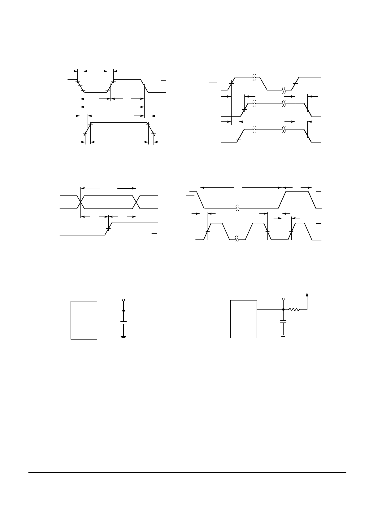
SWITCHING W AVEFORMS
10%
V
DD
GND
1/f
clk
OUTPUT A
(DATA OUT)
CLK
90%
50%
90%
50%
10%
t
PLH
t
PHL
t
TLH
t
THL
t
w
t
w
t
f
t
r
Figure 1.
ENB
OUTPUT A
OUTPUT B
10%
V
DD
GND
50%
50%
t
PLZ
t
PLHtPHL
50%
t
PZL
Figure 2.
D
in
CLK
50%
VALID
50%
t
su
t
h
V
DD
GND
V
DD
GND
Figure 3.
CLK
ENB
50%
t
su
t
h
FIRST
CLK
LAST
CLK
t
rec
50%
Figure 4.
V
DD
GND
V
DD
GND
t
w
t
w
TEST POINT
DEVICE
UNDER
TEST
C
L
*
*Includes all probe and fixture capacitance.
Figure 5. Test Circuit
TEST POINT
DEVICE
UNDER
TEST
C
L
*
*Includes all probe and fixture capacitance.
Figure 6. Test Circuit
V +
7.5 k
Ω
MC145190•MC145191 MOTOROLA
6
LOOP SPECIFICATIONS (V
DD
= VCC = 4.5 to 5.5 V unless otherwise indicated, TA = – 40 to + 85°C)
Figure
Guaranteed
Operating Range
Symbol Parameter Test Condition
Figure
No.
Min Max
Unit
V
in
Input Voltage Range, f
in
100 MHz ≤ fin < 250 MHz
250 MHz ≤ fin ≤ 1100 MHz
7 400
200
1500
1500
mV p–p
f
ref
Input Frequency Range, REF
in
MC145190
Externally Driven in
Reference Mode MC145191
Vin ≥ 400 mV p–p
Vin ≥ 1 V p–p
Vin ≥ 400 mV p–p
Vin ≥ 1 V p–p
8 13
6*
12
4.5*
27
27
27
27
MHz
f
XTAL
Crystal Frequency, Crystal Mode C1 ≤ 30 pF, C2 ≤ 30 pF, Includes
Stray Capacitance
9 2 15 MHz
f
out
Output Frequency, REF
out
CL = 30 pF 10, 12 dc 10 MHz
f Operating Frequency of the Phase Detectors dc 2 MHz
t
w
Output Pulse Width, φR, φV, LD MC145190
MC145191
fR in Phase with fV, CL = 50 pF,
VPD = 5.5 V , VDD = VCC = 5.0 V
11, 12 17 85 ns
t
TLH
,
t
THL
Output Transition Times, LD, φV,
φR— MC145191
CL = 50 pF, VPD = 5.5 V,
VDD = VCC = 5.0 V
11, 12 — 65 ns
C
in
Input Capacitance, REF
in
— 5 pF
*If lower frequency is desired, use wave shaping or higher amplitude sinusoidal signal.
SINE WAVE
GENERATOR
1000 pF
DEVICE
UNDER
TEST
1000 pF
TEST
POINT
V+
V
CC
V
DD
f
in
f
in
GND
OUTPUT A
V
in
50
Ω
*
Figure 7. Test Circuit
(fv)
*Characteristic Impedance
SINE WAVE
GENERATOR
50
Ω
DEVICE
UNDER
TEST
0.01
µ
F
TEST
POINT
V
CC
V
DD
REF
in
GND
OUTPUT A
V
in
Figure 8. Test Circuit — Reference Mode
(fR)
TEST
POINT
REF
out
V+
DEVICE
UNDER
TEST
C1
TEST
POINT
V
CC
V
DD
OUTPUT A
GND
REF
in
REF
out
C2
Figure 9. Test Circuit — Crystal Mode
(fR)
V+
50%
REF
out
1/f REF
out
Figure 10. Switching Waveform
MC145190•MC145191MOTOROLA
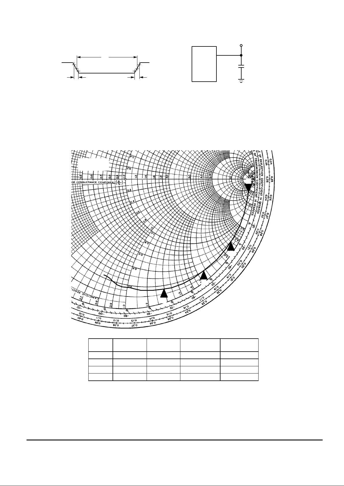
7
10%
90%
OUTPUT
t
TLH
t
THL
Figure 11. Switching Waveform
50%
t
w
TEST POINT
DEVICE
UNDER
TEST
C
L
*
Figure 12. Test Circuit
*Includes all probe and
fixture capacitance.
NORMALIZED INPUT IMPEDANCE AT fin — SERIES FORMAT (R + jX)
(100 MHz to 1.1 GHz)
3
4
2
1
Frequency Resistance Capacitive Capacitance
Marker (MHz) (Ω) Reactance (Ω) (pF)
1 100 338 – 785 2.03
2 500 20.2 – 183 1.74
3 800 11.5 – 109 1.83
4 1100 8.2 – 70.2 2.06
fin (PIN 11)
SOG PACKAGE
MC145190•MC145191 MOTOROLA
8
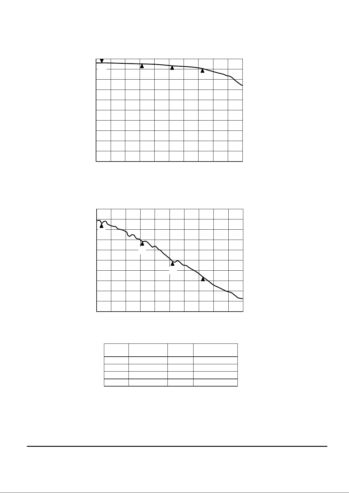
2
3
STAR T 50 MHz STOP 1500 MHz
1
4
RETURN LOSS AT f
in
STAR T 50 MHz STOP 1500 MHz
STANDING WAVE RATIO AT f
in
4
2
3
Frequency Return Loss
Marker (MHz) SWR (dB)
1 100 43.7 0.40
2 500 34.7 0.48
3 800 25.3 0.68
4 1100 17.9 0.98
0 dB
– 5 dB
– 10 dB
51
26
1
1
 Loading...