

Motorola MC145192DT, MC145192F Datasheet
MC145192MOTOROLA
1
$" &
#% %"!&
Includes On–Board 64/65 Prescaler
The MC145192 is a low–voltage single–package synthesizer with serial
interface capable of direct usage up to 1.1 GHz. A special architecture makes
this PLL very easy to program because a byte–oriented format is utilized. Due
to the patented BitGrabber
registers, no address/steering bits are required for
random access
of the three registers. Thus, tuning can be accomplished via a
3–byte serial transfer to the 24–bit A register. The interface is both SPI and
MICROWIRE
compatible.
The device features a single–ended current source/sink phase detector A
output and a double–ended phase detector B output. Both phase detectors
have linear transfer functions (no dead zones). The maximum current of the
single–ended phase detector output is determined by an external resistor tied
from the Rx pin to ground. This current can be varied via the serial port.
The MC145192 phase/frequency detector B φR and φV outputs can be
powered from 2.7 to 5.5 V. This is optimized for 3.0 V systems. The
phase/frequency detector A PD
out
output must be powered from 4.5 to 5.5 V,
and is optimized for a 5 volt supply.
This part includes a differential RF input which may be operated in a
single–ended mode. Also featured are on–board support of an external crystal
and a programmable reference output. The R, A, and N counters are fully
programmable. The C register (configuration register) allows the part to be
configured to meet various applications. A patented feature allows the C
register to shut off unused outputs, thereby minimizing system noise and
interference.
In order to have consistent lock times and prevent erroneous data from being
loaded into the counters, on–board circuitry synchronizes the update of the A
register if the A or N counters are loading. Similarly, an update of the R register
is synchronized if the R counter is loading.
The double–buffered R register allows new divide ratios to be presented to
the three counters (R, A, and N) simultaneously.
• Maximum Operating Frequency: 1100 MHz @ Vin = 200 mV p–p
• Operating Supply Current: 6 mA Nominal at 2.7 V
• Operating Supply Voltage Range (VDD and VCC Pins): 2.7 to 5.0 V
• Operating Supply Voltage Range of Phase Frequency Detector A
(VPD Pin) = 4.5 to 5.5 V
• Operating Supply Voltage Range of Phase Detector B (VPD Pin) = 2.7 to 5.5 V
• Current Source/Sink Phase Detector Output Capability: 2 mA Maximum
• Gain of Current Source/Sink Phase/Frequency Detector Controllable via Serial Port
• Operating Temperature Range: – 40° to 85°C
• R Counter Division Range: (1 and) 5 to 8191
• N Counter Division Range: 5 to 4095
• A Counter Division Range: 0 to 63
• Dual–Modulus Capability Provides Total Division up to 262,143
• High–Speed Serial Interface: 2 Megabits per Second
• Output A Pin, When Configured as Data Out, Permits Cascading of Devices
• Two General–Purpose Digital Outputs — Output A: Totem–Pole (Push–Pull) with Four Output Modes
Output B: Open–Drain
• Power–Saving Standby Feature with Patented Orderly Recovery for Minimizing Lock Times,
Standby Current: 30 µA
• Evaluation Kit Available (Part Number MC145192EVK)
• See Application Note AN1253/D for Low–Pass Filter Design, and
AN1277/D for Offset Reference PLLs for Fine Resolution or Fast Hopping
BitGrabber is a trademark of Motorola Inc. MICROWIRE is a trademark of National Semiconductor Corp.
Order this document
by MC145192/D
SEMICONDUCTOR TECHNICAL DATA
f
in
TEST 2
OUTPUT B
OUTPUT A
CLOCK
12
13
14
15
16
1110
DATA IN
REF
in
V
CC
ENABLE
8
7
6
5
4
3
2
1
TEST 1
Rx
GND
PD
out
φ
V
φ
R
LD
REF
out
9
18
19
20
17
V
PD
f
in
V
DD
PIN ASSIGNMENT
ORDERING INFORMATION
MC145192F SOG Package
MC145192DT TSSOP
F SUFFIX
SOG PACKAGE
CASE 751J
DT SUFFIX
TSSOP
CASE 948D
20
1
20
1
Motorola, Inc. 1998
REV 3
1/98 TN98012200
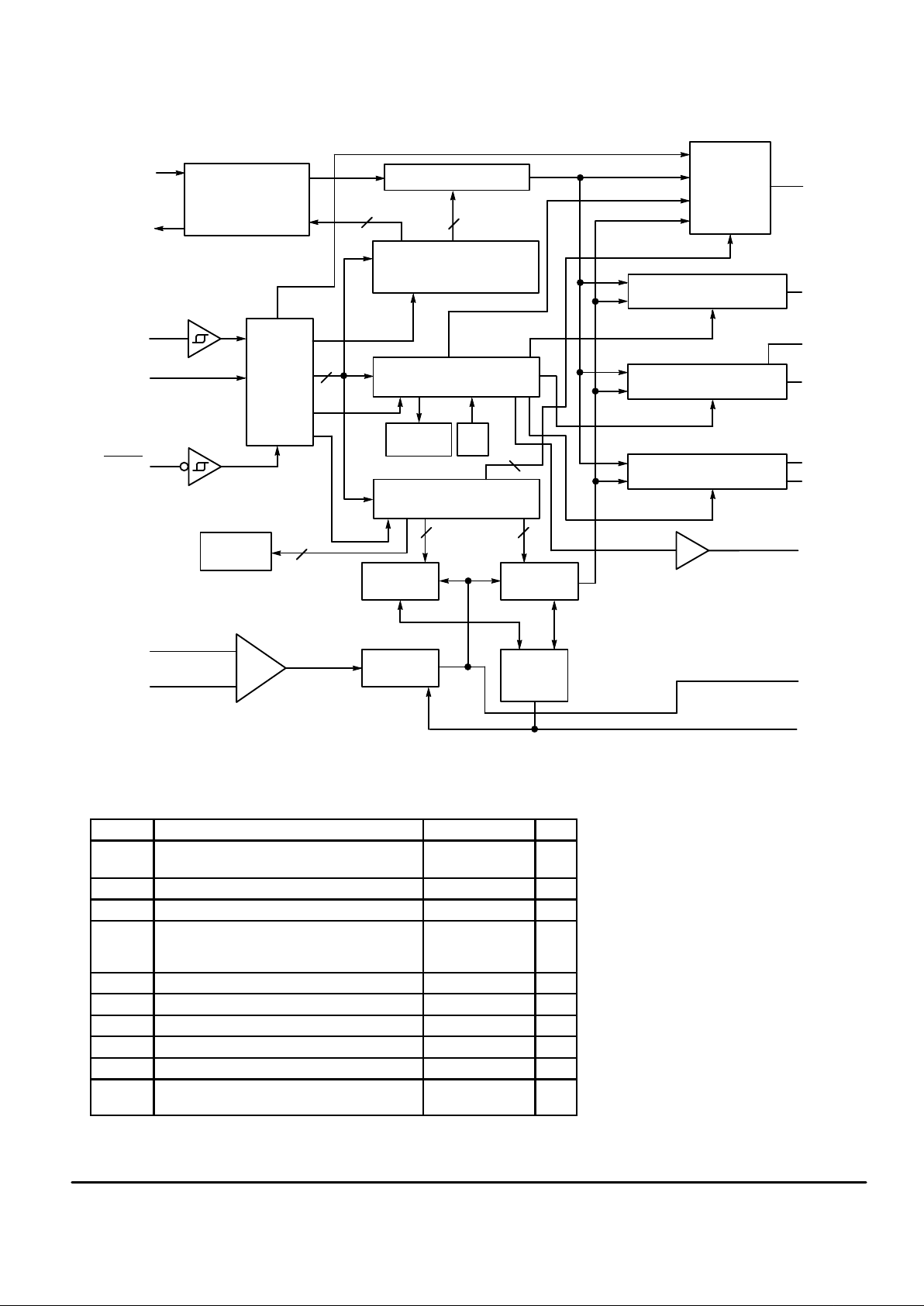
MC145192 MOTOROLA
2
ENABLE
REF
in
DATA IN
CLOCK
REF
out
f
in
f
in
OSC OR
4–STAGE
DIVIDER
(CONFIGURABLE)
20
1
18
19
11
10
OUTPUT A
INPUT
AMP
SELECT
LOGIC
3
13
24
13–STAGE R COUNTER
64/65
PRESCALER
MODULUS
CONTROL
LOGIC
12–STAGE
N COUNTER
6–STAGE
A COUNTER
INTERNAL
CONTROL
SHIFT
REGISTER
AND
CONTROL
LOGIC
STANDBY
LOGIC
POR
BitGrabber
A REGISTER
24 BITS
BitGrabber
C REGISTER
8 BITS
DOUBLE–BUFFERED
BitGrabber
R REGISTER
16 BITS
PHASE/FREQUENCY
DETECTOR B AND CONTROL
PHASE/FREQUENCY
DETECTOR A AND CONTROL
LOCK DETECTOR
AND CONTROL
6 12
4
2
LD
Rx
PD
out
φ
R
φ
V
OUTPUT B
(OPEN–DRAIN
OUTPUT)
TEST 2
TEST 1
9
15
13
4
3
6
8
2
16
SUPPLY CONNECTIONS:
PIN 12 = VCC (V+ TO INPUT AMP AND 64/65 PRESCALER)
PIN 5 = VPD (V+ TO PHASE/FREQUENCY DETECTORS A AND B)
PIN 14 = VDD (V+ TO BALANCE OF CIRCUIT)
PIN 7 = GND (COMMON GROUND)
17
DATA OUT
f
R
f
V
PORT
BLOCK DIAGRAM
MAXIMUM RATINGS*
(Voltages Referenced to GND, unless otherwise stated)
Symbol Parameter Value Unit
VCC,
V
DD
DC Supply Voltage (Pins 12 and 14) – 0.5 to + 6.0 V
V
PD
DC Supply Voltage (Pin 5) VDD – 0.5 to + 6.0 V
V
in
DC Input Voltage – 0.5 to VDD + 0.5 V
V
out
DC Output Voltage,
except Output B, PD
out
, φR, φ
V
Output B, PD
out
, φR, φ
V
– 0.5 to VDD + 0.5
– 0.5 to VPD + 0.5
V
Iin, I
PD
DC Input Current, per Pin (Includes VPD) ± 10 mA
I
out
DC Output Current, per Pin ± 20 mA
I
DD
DC Supply Current, VDD and GND Pins ± 30 mA
P
D
Power Dissipation, per Package 300 mW
T
stg
Storage Temperature – 65 to + 150 °C
T
L
Lead Temperature, 1 mm from Case for
10 Seconds
260 °C
* Maximum Ratings are those values beyond which damage to the device may occur.
Functional operation should be restricted to the limits in the Electrical Characteristics tables
or Pin Descriptions section.
This device contains protection circuitry to
guard against damage due to high static voltages or electric fields. However, precautions
must be taken to avoid applications of any voltage higher than maximum rated voltages to
this high–impedance circuit.
MC145192MOTOROLA
3
ELECTRICAL CHARACTERISTICS (V
DD
= VCC = 2.7 to 5.0 V , Voltages Referenced to GND, TA = – 40° to 85°C, unless otherwise
stated; Phase/Frequency Detector A VPD = 4.5 to 5.5 V with VDD ≤ VPD; Phase/Frequency Detector B VPD = 2.7 to 5.5 V with VDD ≤ VPD)
Symbol
Parameter Test Condition
Guaranteed
Limit
Unit
V
IL
Maximum Low–Level Input Voltage
(Data In, Clock, Enable
, REFin)
Device in Reference Mode, DC Coupled 0.2 x V
DD
V
V
IH
Minimum High–Level Input Voltage
(Data In, Clock, Enable
, REFin)
Device in Reference Mode, DC Coupled 0.8 x V
DD
V
V
Hys
Minimum Hysteresis Voltage
(Clock, Enable
)
VDD = 2.7 V
VDD = 5.0 V
100
300
mV
V
OL
Maximum Low–Level Output Voltage
(REF
out
, Output A)
I
out
= 20 µA, Device in Reference Mode 0.1 V
V
OH
Minimum High–Level Output Voltage
(REF
out
, Output A)
I
out
= – 20 µA, Device in Reference Mode VDD – 0.1 V
I
OL
Minimum Low–Level Output Current
(REF
out
, LD)
V
out
= 0.4 V 0.25 mA
I
OL
Minimum Low–Level Output Current
(φR, φV)
V
out
= 0.4 V
VDD, VPD = 2.7 V
0.36 mA
I
OL
Minimum Low–Level Output Current
(Output A)
V
out
= 0.4 V 0.6 mA
I
OL
Minimum Low–Level Output Current
(Output B)
V
out
= 0.4 V 1.0 mA
I
OH
Minimum High–Level Output Current
(REF
out
, LD)
V
out
= VDD – 0.4 V – 0.25 mA
I
OH
Minimum High–Level Output Current
(φR, φV)
V
out
= VPD – 0.4 V
VDD, VPD = 2.7 V
– 0.36 mA
I
OH
Minimum High–Level Output Current
(Output A Only)
V
out
= VDD – 0.4 V – 0.35 mA
I
in
Maximum Input Leakage Current
(Data In, Clock, Enable
, REFin)
Vin = VDD or GND, Device in XTAL Mode ± 1.0 µA
I
in
Maximum Input Current
(REFin)
Vin = VDD or GND, Device in Reference Mode ± 150 µA
I
OZ
Maximum Output Leakage Current (PD
out
) V
out
= VPD – 0.5 V or 0.5 V, Output in High–Impedance
State
± 200 nA
(Output B) Output in High–Impedance State ± 10 µA
I
STBY
Maximum Standby Supply Current
(VDD + VPD Pins)
Vin = VDD or GND; Outputs Open; Device in Standby
Mode, Shut–Down Crystal Mode or REF
out
–Static–Low
Reference Mode; Output B Controlling VCC per Figure 22
30 µA
I
PD
Maximum Phase Detector
Quiescent Current (VPD Pin)
Bit C6 = High Which Selects Phase Detector A,
PD
out
= Open, PD
out
= Static Low or High, Bit C4 = Low
Which is NOT Standby, IRx = 113 µA, VPD = 5.5 V
600 µA
Bit C6 = Low Which Selects Phase Detector B, φR and
φV = Open, φR and φV = Static Low or High, Bit
C4 = Low Which is NOT Standby
30
I
T
Total Operating Supply Current
(VDD + VPD + VCC Pins)
fin = 1.1 GHz; REFin = 13 MHz @ 1 V p–p;
Output A = Inactive and No Connect; VDD = VCC,
REF
out
, φV, φR, PD
out
, LD = No Connect;
Data In, Enable
, Clock = VDD or GND, Phase Detector A
Off
* mA
*The nominal values are:
6 mA at VDD = 2.7 V and VPD = 2.7 V
9 mA at VDD = 5.0 V and VPD = 5.5 V
These are not guaranteed limits.
MC145192 MOTOROLA
4
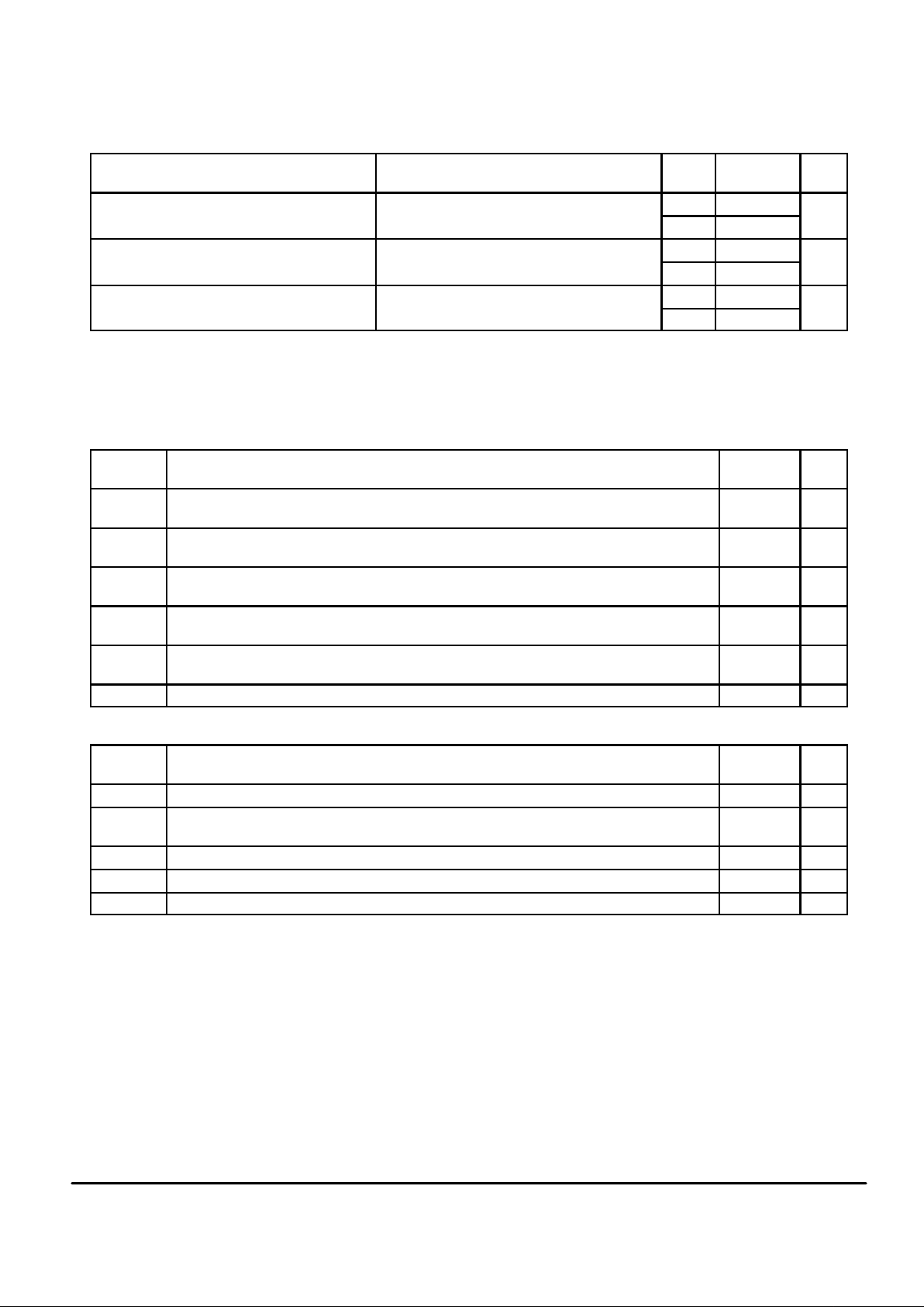
ANALOG CHARACTERISTICS — CURRENT SOURCE/SINK OUTPUT — PD
out
(I
out
≤ 2 mA, VDD = VCC = 2.7 to 5.0 V , Voltages Referenced to GND, VDD = VCC ≤ VPD)
Parameter
Test Condition V
PD
Guaranteed
Limit
Unit
Maximum Source Current Variation Part–to–Part V
out
= 0.5 x V
PD
4.5 ± 20 %
5.5 ± 20
Maximum Sink–versus–Source Mismatch V
out
= 0.5 x V
PD
4.5 12 %
(Note 3) 5.5 12
Output Voltage Range I
out
variation ≤ 20% 4.5 0.5 to 4.0 V
(Note 3) 5.5 0.5 to 5.0
NOTES:
1. Percentages calculated using the following formula: (Maximum Value – Minimum Value)/Maximum Value.
2. See Rx Pin Description for external resistor values.
3. This parameter is guaranteed for a given temperature within – 40° to 85°C.
AC INTERFACE CHARACTERISTICS
(VDD = VCC = 2.7 to 5.0 V , TA = – 40° to 85°C, CL = 50 pF, Input tr = tf = 10 ns, VPD = 2.7 to 5.5 V with VDD ≤ VPD)
Symbol
Parameter
Guaranteed
Limit
Unit
f
clk
Serial Data Clock Frequency (Figure 1)
NOTE: Refer to Clock tw below
dc to 2.0 MHz
t
PLH
,
t
PHL
Maximum Propagation Delay, Clock to Output A (Selected as Data Out) (Figures 1 and 5) 200 ns
t
PLH
,
t
PHL
Maximum Propagation Delay, Enable to Output A (Selected as Port) (Figures 2 and 5) 200 ns
t
PZL
,
t
PLZ
Maximum Propagation Delay, Enable to Output B (Figures 2 and 6) 200 ns
t
TLH
,
t
THL
Maximum Output Transition T ime, Output A and Output B; t
THL
only, on Output B
(Figures 1, 5, and 6)
200 ns
C
in
Maximum Input Capacitance — Data In, Clock, Enable 10 pF
TIMING REQUIREMENTS (V
DD
= VCC = 2.7 to 5.0 V , TA = – 40° to 85°C, Input tr = tf = 10 ns unless otherwise indicated)
Symbol Parameter
Guaranteed
Limit
Unit
tsu, t
h
Minimum Setup and Hold Times, Data In versus Clock (Figure 3) 50 ns
tsu, th,
t
rec
Minimum Setup, Hold and Recovery Times, Enable versus Clock (Figure 4) 100 ns
t
w
Minimum Pulse Width, Enable (Figure 4) * cycles
t
w
Minimum Pulse Width, Clock (Figure 1) 250 ns
tr, t
f
Maximum Input Rise and Fall Times, Clock (Figure 1) 100 µs
*The minimum limit is 3 REFin cycles or 195 fin cycles, whichever is greater.
MC145192MOTOROLA
5
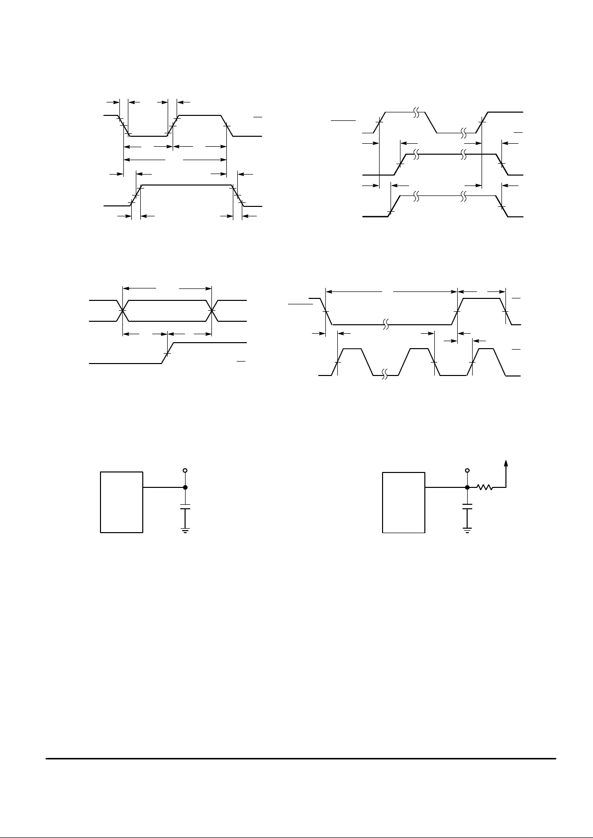
SWITCHING W AVEFORMS
10%
V
DD
GND
1/f
clk
OUTPUT A
(DATA OUT)
CLOCK
90%
50%
90%
50%
10%
t
PLH
t
PHL
t
TLH
t
THL
t
w
t
w
t
f
t
r
Figure 1.
ENABLE
OUTPUT A
OUTPUT B
10%
V
DD
GND
50%
50%
t
PLZ
t
PLHtPHL
50%
t
PZL
Figure 2.
DATA IN
CLOCK
50%
VALID
50%
t
su
t
h
V
DD
GND
V
DD
GND
Figure 3.
CLOCK
ENABLE
50%
t
su
t
h
FIRST
CLOCK
LAST
CLOCK
t
rec
50%
Figure 4.
V
DD
GND
V
DD
GND
t
w
t
w
TEST POINT
DEVICE
UNDER
TEST
CL*
*Includes all probe and fixture capacitance.
Figure 5. Test Circuit
TEST POINT
DEVICE
UNDER
TEST
CL*
*Includes all probe and fixture capacitance.
Figure 6. Test Circuit
+V
PD
7.5 k
MC145192 MOTOROLA
6
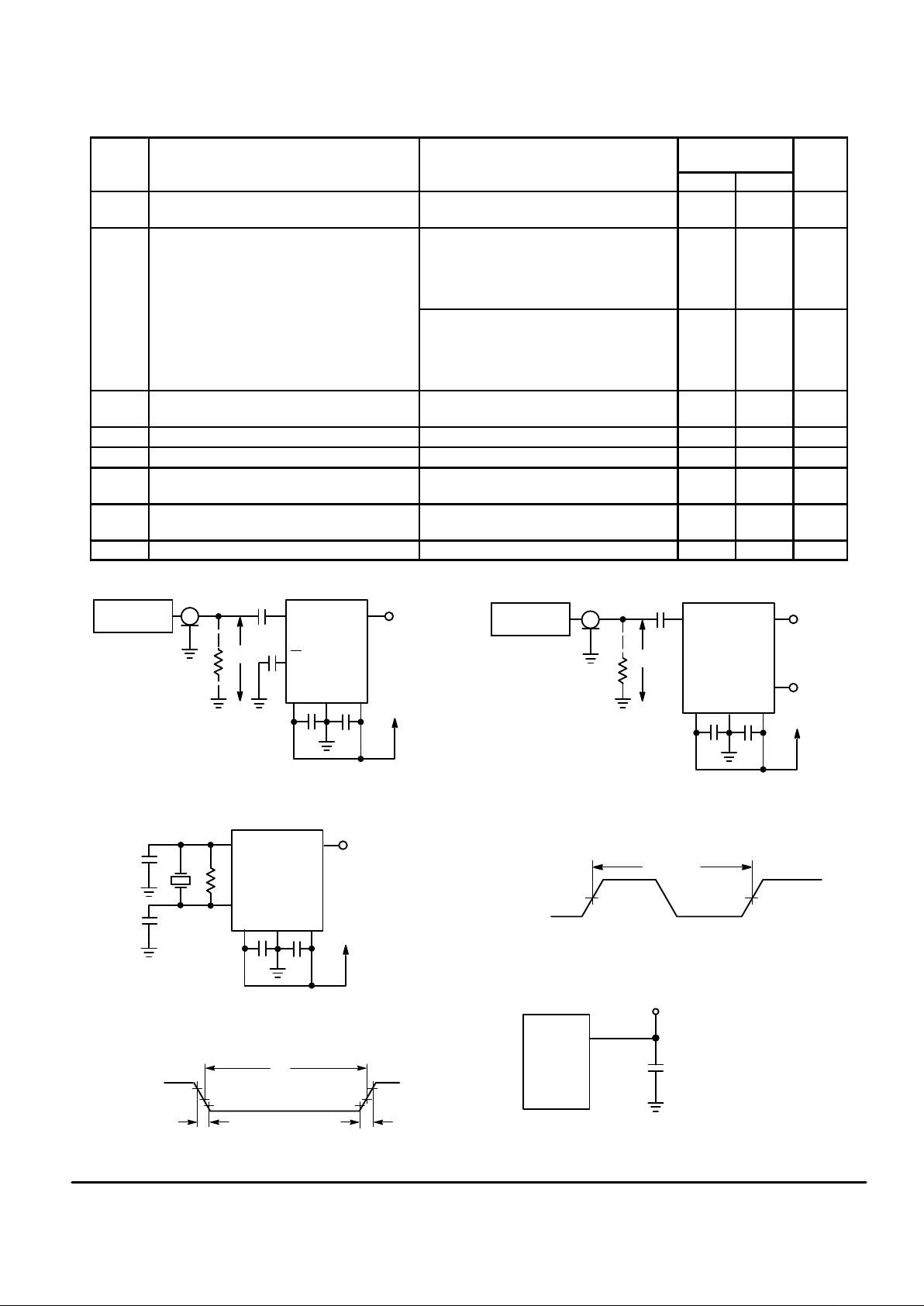
LOOP SPECIFICATIONS (V
DD
= VCC = 2.7 to 5.0 V unless otherwise indicated, TA = – 40° to 85°C)
Guaranteed
Operating Range
Symbol Parameter Test Condition Min Max Unit
V
in
Input Voltage Range, f
in
(Figure 7)
100 MHz ≤ fin < 250 MHz
250 MHz ≤ fin ≤ 1100 MHz
400
200
1500
1500
mV p–p
f
ref
Input Frequency, REFin Externally Driven in
Reference Mode (Figure 8)
Vin ≥ 400 mV p–p
VDD = 2.7 V
VDD = 3.0 V
VDD = 3.5 V
VDD = 4.5 to 5 V
1
4.5
5.5
12
20
20
20
27
MHz
Vin ≥ 1 V p–p
VDD = 2.7 V
VDD = 3.0 V
VDD = 3.5 V
VDD = 4.5 to 5 V
1
1.5
2
4.5
20
20
20
27
MHz
f
XTAL
Crystal Frequency, Crystal Mode
(Figure 9)
C1 ≤ 30 pF, C2 ≤ 30 pF, Includes Stray
Capacitance
2 10 MHz
f
out
Output Frequency, REF
out
(Figures 10 and 12) CL = 30 pF dc 5 MHz
f Operating Frequency of the Phase Detectors dc 1 MHz
t
w
Output Pulse Width, φR, φV, and LD
(Figures 11 and 12)
fR in Phase with fV, CL = 50 pF,
VPD = 2.7 V , VDD = VCC = 2.7 V
20 140 ns
t
TLH
,
t
THL
Output Transition Times, LD, φV, and φ
R
(Figures 11 and 12)
CL = 50 pF, VPD = 2.7 V,
VDD = VCC = 2.7 V
— 80 ns
C
in
Input Capacitance, REF
in
— 5 pF
SINE WAVE
GENERATOR
1000 pF
DEVICE
UNDER
TEST
1000 pF
TEST
POINT
V+
V
CC
V
DD
f
in
f
in
GND
OUTPUT A
V
in
50
Ω
*
Figure 7. Test Circuit
(fv)
*Characteristic Impedance
SINE WAVE
GENERATOR
DEVICE
UNDER
TEST
0.01
µ
F
TEST
POINT
V
CC
V
DD
REF
in
GND
OUTPUT A
V
in
Figure 8. Test Circuit–Reference Mode
(fR)
TEST
POINT
REF
out
V+
DEVICE
UNDER
TEST
C1
TEST
POINT
V
CC
V
DD
OUTPUT A
GND
REF
in
REF
out
C2
Figure 9. Test Circuit–Crystal Mode
(fR)
V+
50%
REF
out
1/f REF
out
Figure 10. Switching Waveform
10%
90%
OUTPUT
t
TLH
t
THL
Figure 11. Switching Waveform
50%
t
w
TEST POINT
DEVICE
UNDER
TEST
CL*
*Includes all probe and
fixture capacitance.
Figure 12. Test Circuit
50
Ω
*
*Characteristic Impedance
MC145192MOTOROLA
7
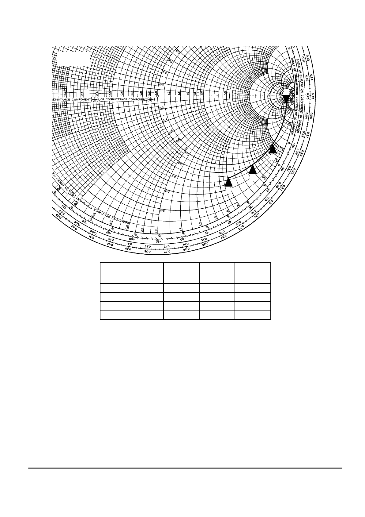
3
2
1
4
fin (PIN 11)
SOG PACKAGE
Marker
Frequency
(MHz)
Resistance
(Ω)
Capacitive
Reactance
(Ω)
Capacitance
(pF)
1 100 574 – 881 1.81
2 500 57.9 – 242 1.31
3 800 38.3 – 148 1.34
4 1100 31.6 – 103 1.40
Figure 13. Normalized Input Impedance at fin — Series Format (R + jX)
(100 MHz to 1100 MHz)

MC145192 MOTOROLA
8
PIN DESCRIPTIONS
DIGITAL INTERFACE PINS
Data In (Pin 19)
Serial Data Input. The bit stream begins with the MSB and
is shifted in on the low–to–high transition of Clock. The bit
pattern is 1 byte (8 bits) long to access the C or configuration
register, 2 bytes (16 bits) to access the first buffer of the R
register, or 3 bytes (24 bits) to access the A register (see
Table 1). The values in the C, R, and A registers do not
change during shifting because the transfer of data to the
registers is controlled by Enable
.
CAUTION
The value programmed for the N–counter must
be greater than or equal to the value of the A–
counter.
The 13 LSBs of the R register are double–buffered. As indicated above, data is latched into the first buffer on a 16–bit
transfer. (The 3 MSBs are not double–buffered and have an
immediate effect after a 16–bit transfer .) The second buffer of
the R register contains the 13 bits for the R counter. This second buffer is loaded with the contents of the first buffer when
the A register is loaded (a 24–bit transfer). This allows presenting new values to the R, A, and N counters simultaneously. If this is not required, then the 16–bit transfer may
be followed by pulsing Enable
low with no signal on the Clock
pin. This is an alternate method of transferring data to the
second buffer of the R register. See Figure 17.
The bit stream needs neither address nor steering bits due
to the innovative BitGrabber registers. Therefore, all bits in
the stream are available to be data for the three registers.
Random access of any register is provided. That is, the registers may be accessed in any sequence. Data is retained in
the registers over a supply range of 2.7 to 5.0 V . The formats
are shown in Figures 15, 16, and 17.
Data In typically switches near 50% of VDD to maximize
noise immunity. This input can be directly interfaced to
CMOS devices with outputs guaranteed to switch near rail–
to–rail. When interfacing to NMOS or TTL devices, either a
level shifter (MC74HC14A, MC14504B) or pull–up resistor of
1kΩ to 10 kΩ must be used. Parameters to consider when
sizing the resistor are worst–case IOL of the driving device,
maximum tolerable power consumption, and maximum data
rate.
Table 1. Register Access
(MSBs are shifted in first, C0, R0, and A0 are the LSBs)
Number
of Clocks
Accessed
Register
Bit
Nomenclature
8
16
24
Other Values ≤ 32
Values > 32
C Register
R Register
A Register
Not Allowed
See Figures 24
to 27
C7, C6, C5, . . ., C0
R15, R14, R13, . . ., R0
A23, A22, A21, . . ., A0
Clock (Pin 18)
Serial Data Clock Input. Low–to–high transitions on Clock
shift bits available at the Data pin, while high–to–low transitions shift bits from Output A (when configured as Data Out,
see Pin 16). The 24–1/2–stage shift register is static,
allowing clock rates down to dc in a continuous or intermittent mode.
Eight clock cycles are required to access the C register.
Sixteen clock cycles are needed for the first buffer of the R
register. Twenty–four cycles are used to access the A register. See Table 1 and Figures 15, 16, and 17. The number of
clocks required for cascaded devices is shown in Figures 25
through 27.
Clock typically switches near 50% of VDD and h as a
Schmitt–triggered input buffer. Slow Clock rise and fall times
are allowed. See the last paragraph of Data In for more
information.
NOTE
To guarantee proper operation of the power–on
reset (POR) circuit, the Clock pin must be held at
GND (with Enable
being a don’t care) or Enable
must be held at the potential of the V+ pin (with
Clock being a don’t care) during power–up. As an
alternative, the bit sequence of Figure 18 may be
used.
Enable
(Pin 17)
Active–Low Enable Input. This pin is used to activate the
serial interface to allow the transfer of data to/from the device. When Enable is in an inactive high state, shifting is inhibited and the port is held in the initialized state. To transfer
data to the device, Enable
(which must start inactive high) is
taken low, a serial transfer is made via Data In and Clock,
and Enable
is taken back high. The low–to–high transition on
Enable transfers data to the C or A registers and first buffer
of the R register, depending on the data stream length per
Table 1.
NOTE
Transitions on Enable
must not be attempted
while Clock is high. This will put the device out of
synchronization with the microcontroller. Resynchronization occurs when Enable
is high and
Clock is low.
This input is also Schmitt–triggered and switches near
50% of VDD, thereby minimizing the chance of loading erroneous data into the registers. See the last paragraph of Data
In for more information.
For POR information, see the note for the Clock pin.
Output A (Pin 16)
Configurable Digital Output. Output A is selectable as fR,
fV, Data Out, or Port. Bits A22 and A23 in the A register control the selection; see Figure 16.
If A23 = A22 = high, Output A is configured as fR. This signal is the buffered output of the 13–stage R counter. The f
R
signal appears as normally low and pulses high. The fR signal can be used to verify the divide ratio of the R counter.
This ratio extends from 5 to 8191 and is determined by the
binary value loaded into bits R0 through R12 in the R register. Also, direct access to the phase detectors via the REF
in
pin is allowed by choosing a divide value of one. See Figure 17. The maximum frequency at which the phase detectors operate is 1 MHz. Therefore, the frequency of fR should
not exceed 1 MHz.
If A23 = high and A22 = low, Output A is configured as fV.
This signal is the buffered output of the 12–stage N counter.
 Loading...