

Motorola MC145018P Datasheet
ÎÎÎ
ÎÎÎ
ÎÎÎ
ÎÎÎ
ÎÎÎ
SEMICONDUCTOR TECHNICAL DATA
# ## %!#
&#
# $#"
High–Performance Silicon–Gate CMOS
The MC54/74HCT374A may be used as a level converter for
interfacing TTL or NMOS outputs to High–Speed CMOS inputs.
The HCT374A is identical in pinout to the LS374.
Data meeting the setup and hold time is clocked to the outputs with the
rising edge of Clock. The Output Enable does not affect the state of the
flip–flops, but when Output Enable is high, the outputs are forced to the
high–impedance state. Thus, data may be stored even when the outputs
are not enabled.
The HCT374A is identical in function to the HCT574A, which has the
input pins on the opposite side of the package from the output pins. This
device is similar in function to the HCT534A, which has inverting outputs.
• Output Drive Capability: 15 LSTTL Loads
• TTL/NMOS–Compatible Input Levels
• Outputs Directly Interface to CMOS, NMOS, and TTL
• Operating Voltage Range: 4.5 to 5.5 V
• Low Input Current: 1.0 µA
• In Compliance with the Requirements Defined by JEDEC Standard
No. 7A
• Chip Complexity: 276 FETs or 69 Equivalent Gates
• Improvements over HCT374
— Improved Propagation Delays
— 50% Lower Quiescent Power
— Improved Input Noise and Latchup Immunity
LOGIC DIAGRAM
3
D0
4
D1
7
D2
8
DATA
INPUTS
OUTPUT ENABLE
Internal Gate Count*
Internal Gate Propagation Delay
Internal Gate Power Dissipation
Speed Power Product
*Equivalent to a two–input NAND gate.
D3
13
D4
14
D5
17
D6
18
D7
11
CLOCK
1
Design Criteria
2
Q0
5
Q1
6
Q2
9
Q3
12
Q4
15
Q5
16
Q6
19
Q7
PIN 20 = V
PIN 10 = GND
CC
Value
69
1.5
5.0
.0075
NONINVERTING
OUTPUTS
Units
ea.
ns
µW
pJ
J SUFFIX
20
1
20
1
20
1
20
1
20
1
ORDERING INFORMATION
MC54HCTXXXAJ
MC74HCTXXXAN
MC74HCTXXXADW
MC74HCTXXXASD
MC74HCTXXXADT
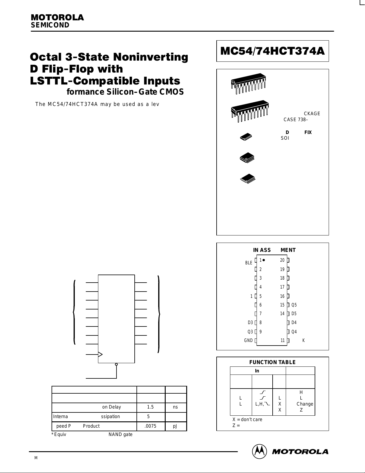
PIN ASSIGNMENT
OUTPUT
ENABLE
Q0
D0
D1
Q1 5
Q2
D2
D3
Q3
GND
FUNCTION TABLE
Inputs Output
Output
Enable Clock D Q
LHH
LLL
L L,H, X No Change
HXXZ
X = don’t care
Z = high impedance
CERAMIC PACKAGE
CASE 732–03
PLASTIC PACKAGE
CASE 738–03
SOIC PACKAGE
CASE 751D–04
SSOP PACKAGE
CASE 940C–03
TSSOP PACKAGE
CASE 948E–02
1
2
3
4
6
7
8
9
10
20
19
18
17
16
15
14
13
12
11
N SUFFIX
DW SUFFIX
SD SUFFIX
DT SUFFIX
Ceramic
Plastic
SOIC
SSOP
TSSOP
V
CC
Q7
D7
D6
Q6
Q5
D5
D4
Q4
CLOCK
2/97
Motorola, Inc. 1997
1
REV 7
MC54/74HCT374A
Î
Î
Î
Î
Î
Î
Î
Î
Î
Î
Î
Î
Î
Î
Î
Î
Î
Î
Î
Î
Î
Î
Î
Î
Î
Î
Î
Î
Î
Î
Î
Î
Î
Î
Î
Î
Î
Î
Î
Î
Î
Î
Î
Î
Î
Î
Î
Î
Î
Î
MAXIMUM RATINGS*
Symbol
V
V
I
I
Î
Î
T
Î
Î
Î
DC Supply Voltage (Referenced to GND)
CC
V
DC Input Voltage (Referenced to GND)
in
DC Output Voltage (Referenced to GND)
out
I
DC Input Current, per Pin
in
DC Output Current, per Pin
out
DC Supply Current, VCC and GND Pins
CC
P
Power Dissipation in Still Air,Plastic or Ceramic DIP†
D
ОООООООООООО
ОООООООООООО
Storage Temperature
stg
ОООООООООООО
T
Lead Temperature, 1 mm from Case for 10 Seconds
L
ОООООООООООО
(Plastic DIP, SOIC, SSOP or TSSOP Package)
ОООООООООООО
*Maximum Ratings are those values beyond which damage to the device may occur.
Functional operation should be restricted to the Recommended Operating Conditions.
†Derating — Plastic DIP: – 10 mW/_C from 65_ to 125_C
Ceramic DIP: – 10 mW/_C from 100_ to 125_C
SOIC Package: – 7 mW/_C from 65_ to 125_C
SSOP or TSSOP Package: – 6.1 mW/_C from 65_ to 125_C
For high frequency or heavy load considerations, see Chapter 2 of the Motorola High–Speed CMOS Data Book (DL129/D).
Parameter
SOIC Package†
SSOP or TSSOP Package†
(Ceramic DIP)
Value
– 0.5 to + 7.0
– 0.5 to VCC + 0.5
– 0.5 to VCC + 0.5
± 20
± 35
± 75
750
500
ÎÎÎÎ
450
ÎÎÎÎ
– 65 to + 150
ÎÎÎÎ
ÎÎÎÎ
260
300
ÎÎÎÎ
Unit
V
V
V
mA
mA
mA
mW
Î
Î
_
C
Î
_
C
Î
Î
This device contains protection
circuitry to guard against damage
due to high static voltages or electric
fields. However, precautions must
be taken to avoid applications of any
voltage higher than maximum rated
voltages to this high–impedance circuit. For proper operation, Vin and
V
should be constrained to the
out
range GND v (Vin or V
Unused inputs must always be
tied to an appropriate logic voltage
level (e.g., either GND or VCC).
Unused outputs must be left open.
) v VCC.
out
RECOMMENDED OPERATING CONDITIONS
Symbol
V
CC
Vin, V
T
A
tr, t
DC Supply Voltage (Referenced to GND)
DC Input Voltage, Output Voltage (Referenced to GND)
out
Operating Temperature, All Package Types
Input Rise and Fall Time (Figure 1)
f
Parameter
Min
4.5
0
– 55
0
DC ELECTRICAL CHARACTERISTICS (Voltages Referenced to GND)
Symbol
ÎÎ
V
IH
ÎÎ
V
IL
ÎÎ
V
OH
ÎÎ
ÎÎÎОООООООÎООООООО
V
OL
ÎÎ
ÎÎÎОООООООÎООООООО
I
in
ООООООО
Minimum High–Level Input
ООООООО
Voltage
Maximum Low–Level Input
Voltage
ООООООО
Minimum High–Level Output
Voltage
ООООООО
Maximum Low–Level Output
ООООООО
Voltage
Maximum Input Leakage Current
Parameter
Test Conditions
ООООООО
V
= 0.1 V or VCC – 0.1 V
out
ООООООО
|I
| v 20 µA
out
V
= 0.1 V or VCC – 0.1 V
out
|I
| v 20 µA
ООООООО
out
Vin = VIH or V
|I
| v 20 µA
out
ООООООО
Vin = VIH or V
|I
| v 6.0 mA
out
Vin = VIH or V
ООООООО
|I
| v 20 µA
out
Vin = VIH or V
|I
| v 6.0 mA
out
IL
IL
IL
IL
Vin = VCC or GND
Max
5.5
V
CC
+ 125
500
Unit
V
V
_
C
ns
V
CC
V
ÎÎ
4.5
ÎÎ
5.5
4.5
5.5
ÎÎ
4.5
5.5
ÎÎ
ÎÎ
4.5
4.5
ÎÎ
5.5
4.5
ÎÎ
5.5
Guaranteed Limit
– 55 to
25_C
ÎÎ
2.0
ÎÎ
2.0
0.8
0.8
ÎÎ
4.4
5.4
ÎÎ
ÎÎ
3.98
0.1
ÎÎ
0.1
0.26
ÎÎ
± 0.1
v
85_C
ÎÎ
2.0
ÎÎ
2.0
0.8
0.8
ÎÎ
4.4
5.4
ÎÎ
ÎÎ
3.84
0.1
ÎÎ
0.1
0.33
ÎÎ
± 1.0
v
125_C
ÎÎ
2.0
ÎÎ
2.0
0.8
0.8
ÎÎ
4.4
5.4
ÎÎ
ÎÎ
3.7
0.1
ÎÎ
0.1
0.4
ÎÎ
± 1.0
Unit
Î
Î
Î
Î
Î
Î
Î
µA
V
V
V
V
MOTOROLA High–Speed CMOS Logic Data
2
DL129 — Rev 6
DC ELECTRICAL CHARACTERISTICS (Voltages Referenced to GND)
Î
Î
Î
Î
Î
Î
Î
Î
Î
Î
Î
Î
Î
Î
Î
Current
Î
V
i
= V
CC
GND, Other Inputs
Î
Î
Î
Î
Î
Î
Î
Î
Î
Î
Î
Î
Î
Î
Î
Î
Î
Î
Î
Î
Î
Î
Î
Î
Î
Î
Î
Î
Î
Î
Î
Î
Î
Î
Î
Î
Î
Î
Î
Î
Î
Î
Î
Î
Î
Î
Î
Î
Î
Î
Î
Î
Î
Î
Î
Î
Î
Î
Î
Î
Symbol
Symbol
I
OZ
ÎÎ
I
CC
ÎÎ
Parameter
Parameter
Maximum Three–State
Leakage Current
ООООООО
Maximum Quiescent Supply
Current (per Package)
ООООООО
Output in High–Impedance State
Vin = VIL or V
V
Vin = VCC or GND
I
Test Conditions
Test Conditions
ООООООО
= VCC or GND
out
= 0 µA
ООООООО
out
IH
V
V
CC
CC
V
V
5.5
ÎÎ
5.5
ÎÎ
Guaranteed Limit
– 55 to
25_C
± 0.5
ÎÎ
ÎÎ
4.0
ÎÎ
ÎÎ
MC54/74HCT374A
v
v
85_C
± 5.0
40
125_C
± 10
ÎÎ
160
ÎÎ
Unit
Unit
µA
Î
µA
Î
∆I
CC
ÎÎÎООООООО
Additional Quiescent Supply
Current
Vin = 2.4 V, Any One Input
or
V
= V
n
l
out
ООООООО
or GND
= 0 µA
Other In
uts
5.5
ÎÎ
≥ –55_C
2.9
ÎÎÎ
25_C to 125_C
2.4
ÎÎÎ
mA
Î
NOTE: 1. Total Supply Current = ICC + Σ∆ICC.
NOTE:Information on typical parametric values can be found in Chapter 2 of the Motorola High–Speed CMOS Data Book (DL129/D).
AC ELECTRICAL CHARACTERISTICS (V
ÎÎÎОООООООООООООООООÎОООООООО
ÎÎ
Symbol
f
max
ÎÎ
t
PLH
t
PHL
ÎÎ
t
PLZ
t
PHZ
t
PZL
ÎÎ
t
PZH
t
TLH
t
THL
ÎÎ
C
C
out
ООООООООООООООООО
Maximum Clock Frequency (50% Duty Cycle)
ООООООООООООООООО
(Figures 1 and 4)
,
Maximum Propagation Delay, Clock to Q
(Figures 1 and 4)
ООООООООООООООООО
,
Maximum Propagation Delay, Output Enable to Q
(Figures 2 and 5)
,
Maximum Propagation Delay, Output Enable to Q
ООООООООООООООООО
(Figures 2 and 5)
,
Maximum Output Transition Time, Any Output
(Figures 1 and 4)
ООООООООООООООООО
in
Maximum Input Capacitance
Maximum Three–State Output Capacitance
(Output in High–Impedance State)
= 5.0 V ± 10%, CL = 50 pF, Input tr = tf = 6.0 ns)
CC
Parameter
Guaranteed Limit
– 55 to
ÎÎ
25_C
30
ÎÎ
31
ÎÎ
30
30
ÎÎ
12
ÎÎ
10
15
ÎÎ
v
85_C
24
ÎÎ
39
ÎÎ
38
38
ÎÎ
15
ÎÎ
10
15
ÎÎ
v
125_C
20
ÎÎ
47
ÎÎ
45
45
ÎÎ
18
ÎÎ
10
15
Î
Î
Unit
MHz
Î
Î
Î
Î
pF
pF
ns
ns
ns
ns
NOTE:For propagation delays with loads other than 50 pF , and information on typical parametric values, see Chapter 2 of the Motorola High–
Speed CMOS Data Book (DL129/D).
C
PD
Power Dissipation Capacitance (Per Flip–Flop)*
*Used to determine the no–load dynamic power consumption: PD = CPD V
Motorola High–Speed CMOS Data Book (DL129/D).
TIMING REQUIREMENTS (V
ÎÎ
Symbol
t
su
ÎÎ
t
h
t
w
ÎÎ
tr, t
ÎÎ
High–Speed CMOS Logic Data
DL129 — Rev 6
ООООООООООООООООО
Minimum Setup Time, Data to Clock
ООООООООООООООООО
Minimum Hold Time, Clock to Data
Minimum Pulse Width, Clock
ООООООООООООООООО
Maximum Input Rise and Fall Times
f
ООООООООООООООООО
(Figure 3)
(Figure 3)
(Figure 1)
(Figure 1)
= 5.0 V ± 10%, Input tr = tf = 6.0 ns)
CC
Parameter
Typical @ 25°C, VCC = 5.0 V
65
2
f + ICC VCC. For load considerations, see Chapter 2 of the
CC
pF
Guaranteed Limit
– 55 to
ÎÎ
25_C
12
ÎÎ
5.0
12
ÎÎ
500
ÎÎ
ÎÎ
v
85_C
15
ÎÎ
5.0
15
ÎÎ
500
ÎÎ
ÎÎ
v
125_C
18
ÎÎ
5.0
18
ÎÎ
500
ÎÎ
Î
Unit
Î
Î
Î
ns
ns
ns
ns
3 MOTOROLA
 Loading...