

查询MC141800AT供应商
MOTOROLA
SEMICONDUCTOR TECHNICAL DATA
Product Preview
LCD Segment / Common Driver
CMOS
MC141800A is a CMOS LCD Driver which consists of 193 high voltage
LCD driving signals to drive 128 Segment and 65 Common display. It has
6800-series parallel, IIC serial interface and Serial Peripheral interface (SPI)
capability for operating with general MCU. Besides the general LCD driver
features, it has on chip LCD Smart Bias Divider circuit such that minimize
external component required in applications.
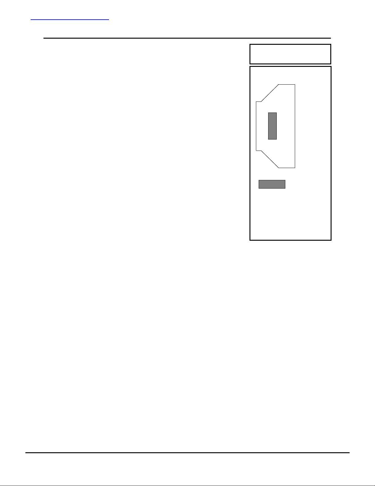
MC141800AT: TAB (Tape Automated Bonding)
MCC141800AZ: Gold Bump Die
• Single Supply Operation, 2.4 V - 3.5 V
• Maximum 16.5V LCD Driving Output Voltage
• Low Current Stand-by Mode (<1uA)
• On Chip Internal DC/DC Converter / External Power Supply
• Smart Bias Divider
• 4X / 5X DC-DC Converter
• 8 bit 6800-series Parallel Interface, 1 MHz IIC Serial Interface and
Serial Peripheral Interface (SPI)
• On chip Oscillator
• Graphic Mode Operation
• On Chip 128 x 65 Display Data RAM
• Master Clear RAM
• Low Power Icon Mode (128 icons, <25uA)
• Display Masks for Implementation of Blinking Effect
• 1 to 65 Selectable Multiplex Ratio
• 1:7 / 1:9 Bias Ratio
• Re-mapping of Row and Column Drivers
• 16 level Internal Contrast Control
• External Contrast Control
• Built-in Temperature Compensation Circuit
• Selectable Display Waveform: Type B or Type C Waveform
• 2V Icon Mode Display On
MC141800A
MC141800AT
TAB
MCC141800AZ
Gold bump die
ORDERING INFORMATION
MC141800AT 70 mm TAB
MCC141800AZ Gold Bump Die
This document contains information on a product under development. Motorola reserves the right to change or discontinue this product without notice.
REV O
2/97
MC141800AMOTOROLA
3–277
Com0 to
Com64
Block Diagram
Seg0~Seg127
OSC1
OSC2
Display
Timing
Generator
HV Buffer Cell Level Shifter
65 Bit
Latch
128 Bit Latch
GDDRAM
65 x 128Bits
Command Decoder
Level
Selector
LCD Driving
Voltage Generator
4x and 5x
DC/DC Converter,
Voltage Regulator,
Smart Bias Divider,
Contrast Control,
Temperature
Compensation
VLL6
VLL2
VCC
VR
VF
C1P
C3P
C1N
C3N
AVDD
AVSS
DVSS
DVDD
MC141800A
3–278
RES
D/
CCE S/P
Parallel / Serial InterfaceCommand Interface
R/
W
CLK
D0~D7
MOTOROLA
COM31
DUMMY
236
COM30
COM29
235
234
COM28
COM27
233
232
COM2
COM1
207
206
COM0
COM64B
205
204
SEG127
SEG126
SEG125
203
202
201
SEG124
SEG123
200
199
SEG66
SEG65
142
141
SEG64
SEG63
140
139
SEG62
SEG61
138
137
SEG2
SEG1
SEG0
COM32
7877767574
COM33
COM34
73
COM61
COM62
464544
COM63
COM64A
43
DUMMY
1234567891011121314151617181920212223242526272829303132333435363738394041
P
C
W
D6
DUMMY
S/
DVDD
RES
D5
SPI
D/
R/
D7/IIC/
D2/A2
D3/Din
D4/Dout
D1/A1
D0/SDA
CEVFVR
CLK
C1P
C1N
C2P
C2N
C3P
C3N
NC
NC
VLL2
VLL3
NCNCNC
NC
VLL4
VLL5
VLL6
OSC1
DVSS
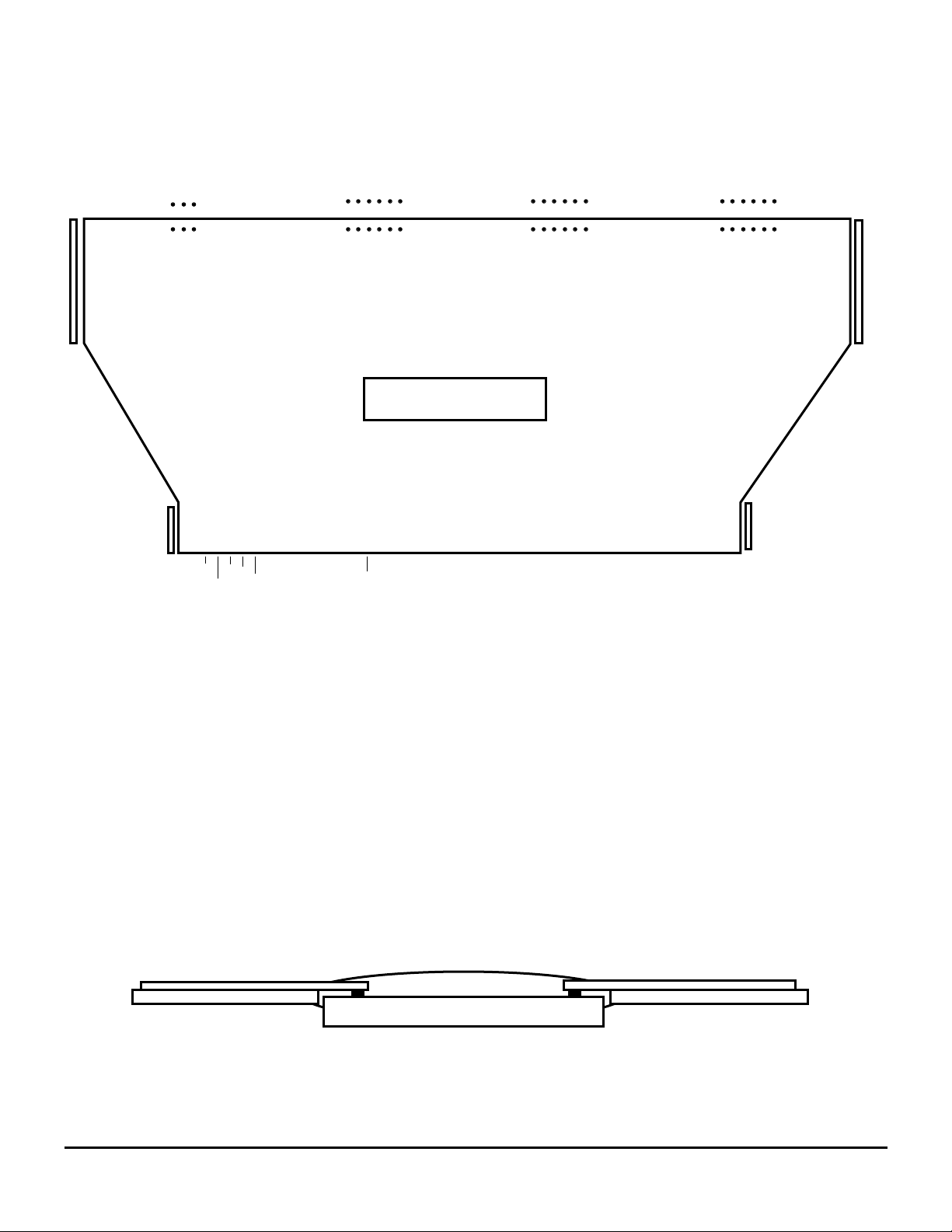
MC141800AT PIN ASSIGNMENT
(COPPER VIEW)
ENCAPSULANT
NC
NC
VCC
AVSS
42
OSC2
AVDD
COPPER
DUMMY
DIE
Mirror Design TAB
POLYIMIDE
MC141800AMOTOROLA
3–279
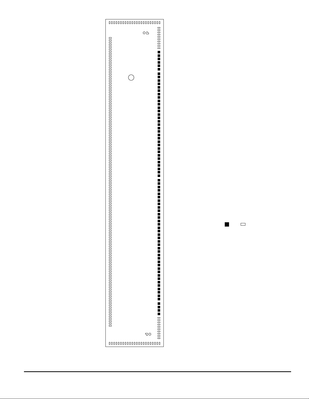
Die Pad Layout for MC141800A
SEG0
SEG1
SEG2
SEG126
SEG127
COM32
COM33...........COM53
.
.
.
.
.
.
.
.
.
.
.
.
.
.
.
.
.
.
.
.
.
.
.
.
.
.
.
.
.
.
.
.
.
.
.
.
.
.
.
.
.
.
.
.
.
.
.
.
.
.
.
.
.
.
.
.
.
.
.
.
.
.
.
.
.
.
.
.
.
.
.
.
.
.
.
.
.
MC141800A
M
COM54
COM55
COM56
.
.
COM63
COM64A
DVSS
DVSS
DVSS
DVSS
DVSS
DVSS
AVDD
OSC2
AVSS
VCC
VCC
DVSS
DVSS
OSC1
DVSS
VLL6
VLL6
VLL5
VLL5
VLL4
VLL4
VLL3
VLL3
VLL2
VLL2
C3N
C3P
C2N
C2P
C1N
C1P
VR
VF
AVSS
AVSS
AVDD
AVDD
DVSS
DVSS
DVDD
DVDD
CE
CLK
CLK
D0
D0
D1
D2
D3
D4
D5
D6
D7
R/W
DVSS
DVSS
DVSS
DVSS
DVSS
DVSS
DVSS
DVSS
DVSS
DVSS
DVSS
DVSS
DVSS
DVSS
DVSS
DVSS
DVSS
DVSS
DVSS
D/C
RES
S/P
DVDD
COM31
.
.
.
.
.
COM22
Input Pad, 65 x 65 (um)
Gold Bump Size :
Output Pad, 42 x 100 (um)
MC141800A
3–280
...........
COM0
COM64B
COM20
COM21
MOTOROLA
MAXIMUM RATINGS* (Voltages Referenced to V
, TA=25˚C)
SS
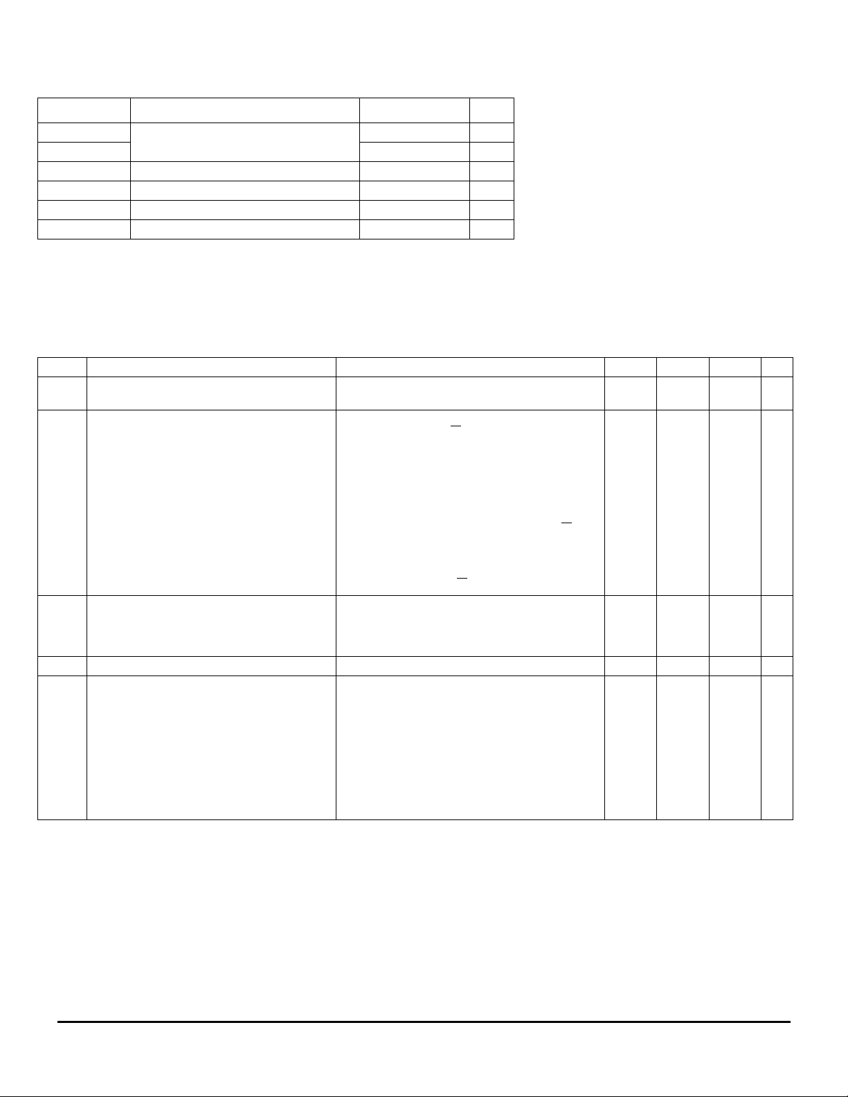
Symbol Parameter Value Unit
AV
,DV
DD
V
CC
V
in
I Current Drain Per Pin Excluding VDD and V
T
A
T
stg
Supply Voltage -0.3 to +4.0 V
DD
VSS-0.3 to VSS+16.5 V
Input Voltage VSS-0.3 to VDD+0.3 V
SS
25 mA
Operating Temperature -30 to +85 ˚C
Storage Temperature Range -65 to +150 ˚C
This device contains circuitry to protect the inputs
against damage due to high static voltages or electric fields; however, it is advised that normal precautions to be taken to avoid application of any voltage
higher than maximum rated voltages to this high
impedance circuit. For proper operation it is recommended that V
and V
in
range VSS < or = (Vin or V
be constrained to the
out
) < or = VDD. Reliability
out
of operation is enhanced if unused input are connected to an appropriate logic voltage level (e.g.,
either VSS or VDD). Unused outputs must be left
open. This device may be light sensitive. Caution
should be taken to avoid exposure of this device to
* Maximum Ratings are those values beyond which damage to the device may occur. Functional
operation should be restricted to the limits in the Electrical Characteristics tables or Pin Descrip-
any light source during normal operation. This
device is not radiation protected.
tion section.
VSS = AVSS = DVSS (DVSS = VSS of Digital circuit, AVSS = VSS of Analogue Circuit)
VDD = AVDD = DVDD (DVDD = VDD of Digital circuit, AVDD = VDD of Analogue Circuit)
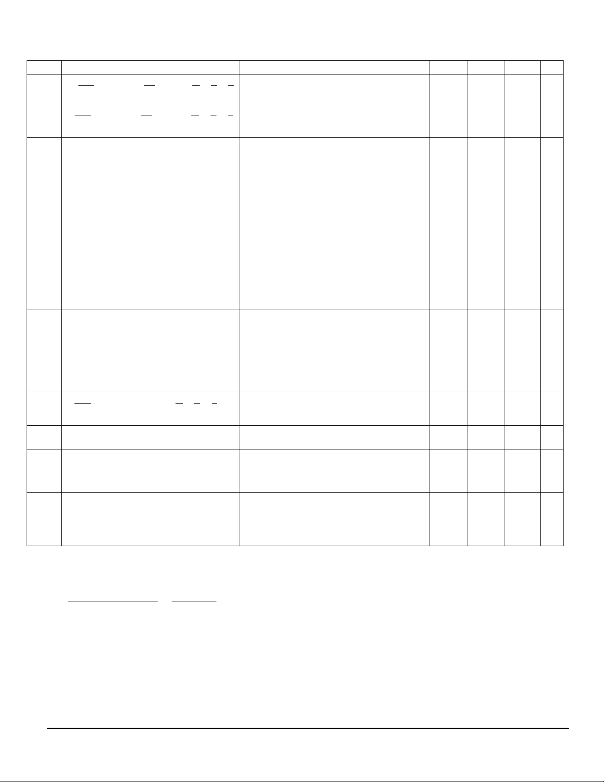
ELECTRICAL CHARACTERISTICS (Voltage Referenced to VSS, VDD=2.4 to 3.5V, TA=25˚C)
Symbol Parameter Test Condition Min Typ Max Unit
DV
AV
Logic Circuit Supply Voltage Range
DD
Voltage Generator Circuit Supply Voltage Range
DD
I
Access Mode Supply Current Drain
AC
(AVDD + DVDD Pins)
I
Display Mode Supply Current Drain
DP
(AVDD + DVDD Pins)
(Absolute value referenced to VSS) 2.4
2.4
VDD=3.0V, Internal DC/DC Converter On, 5X DC/DC
Converter Enabled, R/W accessing, T
=1MHz,
cyc
Osc. Freq.=50KHz, Display On.
VDD=3.0V, Internal DC/DC Converter On, 5X Converter Enabled, R/W Halt, Osc. Freq.=50KHz, Display On.
3.0
-
-
-
500
300
3.5
3.5
TBD
TBD
V
V
µA
µA
I
SB
I
ICON
V
CC
V
LCD
V
ICON
V
OH1
V
OL1
V
R1
V
R2
Standby Mode Supply Current Drain
VDD=3.0V, Display off, Oscillator Disabled, R/W halt.
-
TBD
1
µA
(AVDD + DVDD Pins)
Icon Mode Supply Current Drain
(AVDD + DVDD Pins)
LCD Driving Internal DC/DC Converter Output
(VCC Pin)
LCD Driving Voltage Input (VCC Pin)
VDD=3.0V, Internal Oscillator, Oscillator Enabled,
Display On, Icon On, R/W halt, Freq.=50KHz.
Display On, DC/DC Converter Enabled, Osc. Freq.=
50KHz, Internal Regulator Enabled, Divider Enabled.
Internal DC/DC Converter Disabled.
-
7
7
TBD
15
15
25
16.5
16.5VV
µA
Low Power Icon mode Voltage -2-V
Output High Voltage
I
out
=100µA
0.9*V
DD
-
V
DD
V
(D0-D7, OSC2)
Output Low Voltage
I
out
=100µA
0
-
0.1*V
DD
V
(D0-D7, OSC2)
LCD Driving Voltage Source (VR Pin)
Internal Regulator Enabled (VR voltage depends on
0
-
VCC-0.5
V
Int/Ext Contrast Control)
LCD Driving Voltage Source (VR Pin)
Internal Regulator Disable.
-
Floating
-
V
MC141800AMOTOROLA
3–281
ELECTRICAL CHARACTERISTICS (Voltage Referenced to VSS, VDD=2.4 to 3.5V, TA=25˚C)
Symbol Parameter Test Condition Min Typ Max Unit
V
Input high voltage
IH1
(RES, OSC2, CLK, CE, D0-D7,R/W, D/C, S/P,
OSC1)
V
Input Low voltage
IL1
(RES, OSC2, CLK, CE, D0-D7, R/W, D/C, S/P,
OSC1)
V
LCD Display Voltage Output
LL6
V
LL5
V
LL4
V
LL3
V
LL2
V
LL6
V
LL5
V
LL4
V
LL3
V
LL2
V
LL6
V
LL5
V
LL4
V
LL3
V
LL2
I
OH
(V
, V
LL6
LCD Display Voltage Output
(V
, V
LL6
LCD Display Voltage Input
(V
, V
LL6
Output High Current Source
(D0-D7, OSC2)
LL5
LL5
LL5
, V
, V
, V
LL4
LL4
LL4
, V
, V
, V
LL3
LL3
LL3
, V
, V
, V
LL2
LL2
LL2
Pins)
Pins)
Pins)
Smart Bias Divider Enabled, 1:9 bias ratio
Smart Bias Divider Enabled, 1:7 bias ratio
External Voltage Generator, Smart Bias Divider Disable
V
out=VDD
-0.4V
0.8*V
50
DD
0
-
-
-
-
-
-
-
-
-
-
7
0
0
0
0
-
-
V
8/9*V
7/9*V
2/9*V
1/9*V
V
6/7*V
5/7*V
2/7*V
1/7*V
-
-
-
-
-
-
V
DD
0.2*V
DD
R
R
-
-
R
-
R
-
R
-
R
-
-
R
-
R
-
R
-
R
V
CC
V
LL6
V
LL5
V
LL4
V
LL3
-
V
V
V
V
V
V
V
V
V
V
V
V
V
V
V
V
V
µA
I
Output Low Current Drain
OL
(D0-D7, OSC2)
I
Output Tri-state Current Drain Source
OZ
(D0-D7, OSC2)
IIL/IIHInput Current
(RES, OSC2, CLK, D0-D7, R/W, D/C, S/P,
OSC1)
C
Input Capacitance
IN
(OSC1, OSC2, all logic pins)
V
Internal Contrast Control
CN
(VR Output Voltage)
Temperature Coefficient Compensation
PTC0
PTC1
PTC2
PTC3
Flat Temperature Coefficient
Temperature Coefficient 1*
Temperature Coefficient 2*
Temperature Coefficient 3*
* The formula for the temperature coefficient is:
TC(%)=
VR at 50˚C - VR at 0˚C
50˚C - 0˚C
X
VR at 25˚C
V
out
=0.4V
-
-1
-
-
-50
1
µA
µA
-1 - 1 µA
- 5 7.5 pF
Internal Regulator Enabled, Internal Contrast control
- ± 12 - %
Enabled. (16 Voltage Levels Controlled by Software.
Each level is typically 1.5% of the Internal Regulator
Output Voltage.)
(TC1=0, TC2=0, Internal Regulator Disabled.)
(TC1=0, TC2=1, Internal Regulator Enabled.)
(TC1=1, TC2=0, Internal Regulator Enabled.)
(TC1=1, TC2=1, Internal Regulator Enabled.)
1
X100%
-
-
-
-
0.0
-0.18
-0.22
-0.35
-
%
-
%
-
%
-
%
MC141800A
3–282
MOTOROLA
AC ELECTRICAL CHARACTERISTICS (TA=25˚C, Voltage referenced to VSS, AVDD=DVDD=3V)
Symbol Parameter Test Condition Min Typ Max Unit
F
F
Oscillation Frequency of Display timing generator 60Hz Frame Frequency
OSC
Either External Clock Input or Internal Oscillator
Enabled
Frame Frequency Graphic Display Mode, Normal Frequency Mode,
FRM
65 - 49 MUX
45 60 55 KHz
-
F
OSC
-
15 * MUX
Hz
OSC Internal Oscillation Frequency with different value
of feedback resistor
Graphic Display Mode, Half Frequency Mode,
65 - 49 MUX
Graphic Display Mode, Normal Frequency Mode,
48 - 33 MUX
Graphic Display Mode, Half Frequency Mode,
48 - 33 MUX
Graphic Display Mode, Normal Frequency Mode,
32 - 2 MUX
Graphic Display Mode, Half Frequency Mode,
32 -2 MUX
6-Phase Low Power Icon Mode, Normal Frequency
Mode
6-Phase Low Power Icon Mode, Half Frequency
Mode
4-Phase Low Power Icon Mode, Normal Frequency
Mode
4-Phase Low Power Icon Mode, Half Frequency
Mode
Internal Oscillator Enabled, VDD within operation
range
-
F
OSC
-
30 * MUX
-
F
OSC
-
23 * MUX
F
-
-
OSC
46 * MUX
F
OSC
-
-
30 * MUX
F
-
-
OSC
60 * MUX
F
OSC
-
-
960
-
F
OSC
-
1920
-
F
OSC
-
1024
-
F
OSC
-
2048
See Figure 1 for the relationship
Hz
Hz
Hz
Hz
Hz
Hz
Hz
Hz
Hz
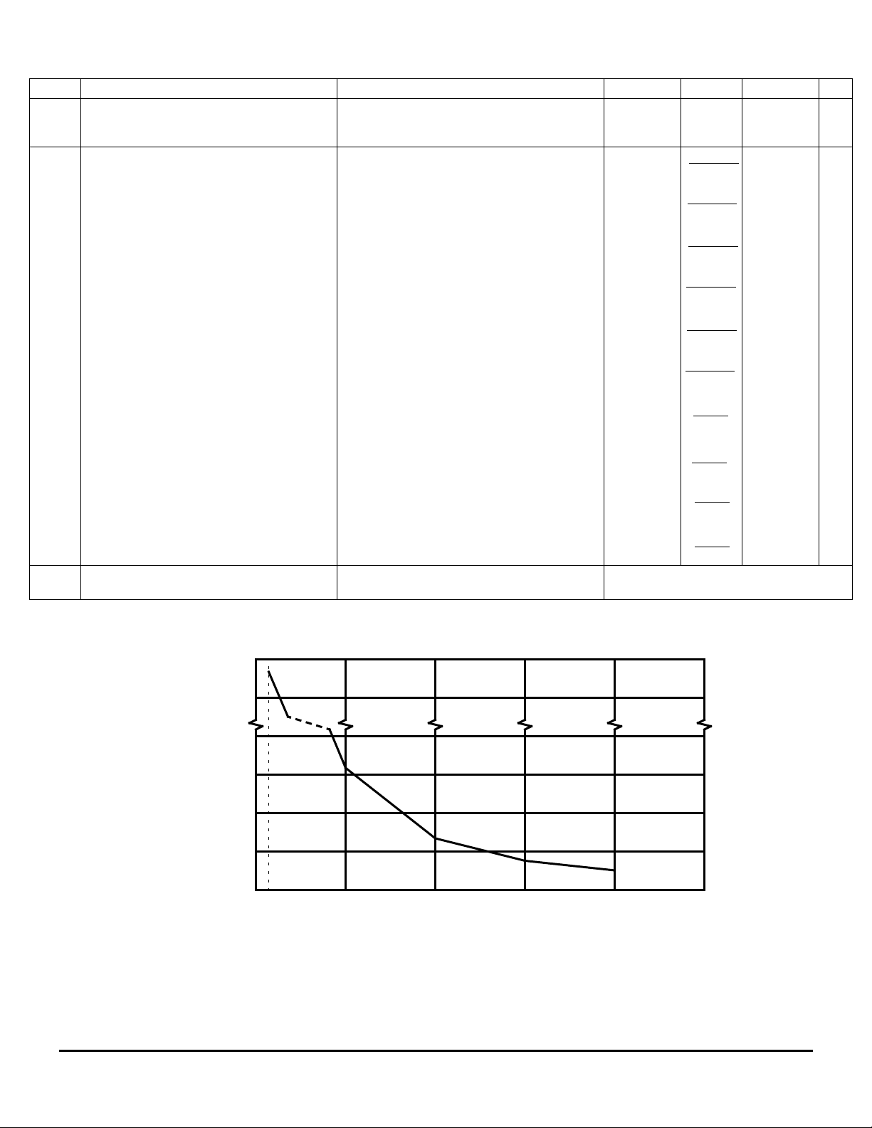
Oscillation
Frequency
(Hz)
280k
260k
90k
70k
50k
30k
10k
100k 500k 1.0M 1.5M 2.0M
Resistor Value between OSC1 and OSC2 (Ω)
Figure 1. Internal Oscillator Frequency Relationship with External Resistor Value
MC141800AMOTOROLA
3–283
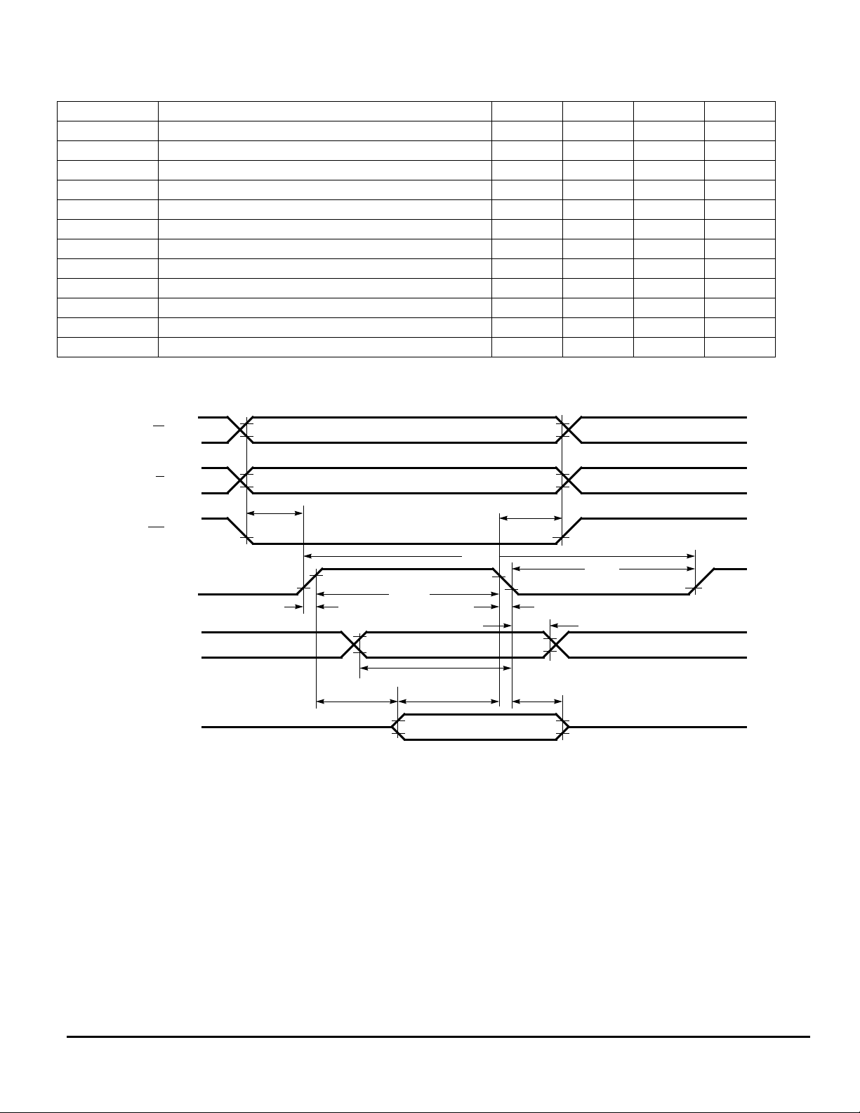
TABLE 3. Parallel Timing Characteristics (TA=-30 to 85˚C, DVDD=2.4 to 3.5V, VSS=0V)
Symbol Parameter Min Typ Max Unit
t
cycle
t
t
DSW
t
DHW
t
DSR
t
DHR
t
ACC
PW
PW
t
AS
AH
EL
EH
t
R
t
F
Clock Cycle Time 1000 - - ns
Address Setup Time 90 - - ns
Address Hold Time 60 - - ns
Write Data Setup Time 210 - - ns
Write Data Hold Time 75 - - ns
Read Data Setup Time 250 - - ns
Read Data Hold Time 75 - - ns
Access Time - - 250 ns
Enable Low Pulse Width 390 - - ns
Enable High Pulse Width 390 - - ns
Rise Time - - 45 ns
Fall Time - - 45 ns
R/W
D/
C
CE
CLK
D0-D7
(Write data to driver)
D0-D7
(Read data from driver)
t
AS
t
cycle
t
AH
PW
PW
t
R
EH
t
F
t
DHW
Valid Data
t
DSW
t
ACC
t
DSR
t
DHR
Valid Data
Figure 2. Parallel 6800-series Interface Timing Characteristics
EL
MC141800A
3–284
MOTOROLA
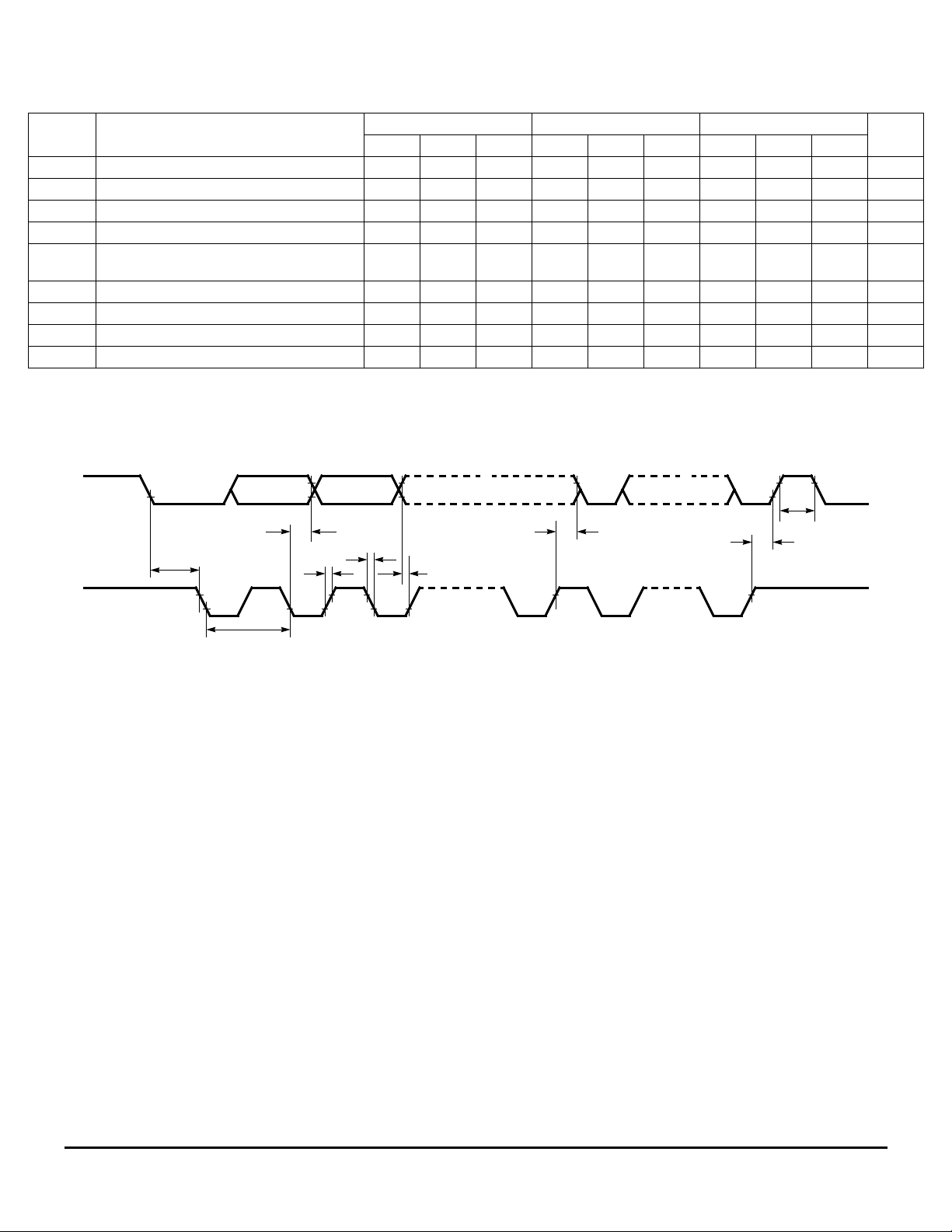
TABLE 4. IIC Serial Timing Characteristics (TA=-30 to 85˚C, DVDD=2.4 to 3.5V, VSS=0V)
100kHz 400kHz 1MHz
Symbol Parameter
t
cycle
t
HSTART
t
t
t
SSTART
Clock Cycle Time 10 - - 2.5 - - 1 - - µs
Start condition Hold Time 4.0 - - 0.6 - - 0.3 - - µs
Data Hold Time 500 - - 300 - - 150 - - ns
HD
Data Setup Time 250 - - 100 - - 50 - - ns
SD
Start condition Setup Time (Only relevant for a
repeated Start condition)
t
SSTOP
t
IDLE
Stop condition Setup Time 4.0 - - 0.6 - - 0.3 - - µs
t
Rise Time for data and clock pin - - 1000 - - 300 - - 150 ns
R
t
Fall Time for data and clock pin - - 300 - - 300 - - 150 ns
F
Idle Time before a new transmission can start 4.7 - - 1.3 - - 0.6 - - µs
Min Typ Max Min Typ Max Min Typ Max
4.7 - - 0.6 - - 0.3 - - µs
Unit
SDA
CLK
t
HSTART
t
cycle
()(
)
t
HD
t
F
t
t
R
SD
t
SSTART
()(
)
t
IDLE
t
SSTOP
Figure 3. IIC Serial Interface Timing Characteristics
MC141800AMOTOROLA
3–285
P
STOP
CONDITION
P
STOP
CONDITION
ACK
)
)
(
)
(
(
)
(
)
(
)
(
)
(
)
(
)
(
)
(
)
(
)
(
9
ACK
)
(
)
(
)
(
)
(
)
(
)
(
1 - 8
DATA
)
(
)
(
)
(
)
(
)
(
)
(
ACK
CR/W
D/
(A0)
9
1 - 8
ACK
ACK
DATA
ACK
CR/W
D/
(A0)
SDA
(From controller)
SDA
(From Driver)
A1
A2
Figure 4. IIC Serial Interface Input Protocol (Write Data to Driver)
ADDRESS
23456789
1
S
START
CONDITION
CLK
SDA
SDA
(From controller)
(From Driver)
A1
A2
ADDRESS
Figure 5. IIC Serial Interface Output Protocol (Read Data from Driver)
23456789
1
S
START
CONDITION
CLK
MC141800A
3–286
MOTOROLA

TABLE 5. SPI Timing Characteristics (TA=-30 to 85˚C, DVDD=2.4 to 3.5V, VSS=0V)
Symbol Parameter Min Typ Max Unit
t
cycle
t
LEAD
t
LAG
t
DSW
t
DHW
t
DVR
t
DHR
t
ACC
t
DIS
t
CLKL
t
CLKH
t
R
t
F
Clock Cycle Time 1000 - - ns
Enable Lead Time 500 - - ns
Enable Lag Time 500 - - ns
Write Data Setup Time 100 - - ns
Write Data Hold Time 100 - - ns
Read Data Valid Time - - 240 ns
Read Data Hold Time 10 - - ns
Access Time - - 120 ns
Disable Time - - 240 ns
Clock Low Time 380 - - ns
Clock High Time 380 - - ns
Rise Time - - 100 ns
Fall Time - - 100 ns
CE
CLK
Dout
Din
t
ACC
t
LEAD
t
CLKH
t
DSW
t
F
t
CLKL
t
cyc
t
DVR
MSB
t
DHW
MSB
Figure 6. SPI Timing Characteristics
)
()(
t
R
)
()(
)
()(
)
()(
t
)
()(
)
()(
DHR
t
LAG
LSB
LSB
t
DIS
MC141800AMOTOROLA
3–287

PIN DESCRIPTIONS
S/P (Serial / Parallel Interface)
This pin is an input pin. The pin is sampled out when reset to
determine what type of interface is desired. The S/P pin input HIGH
for serial interface while input LOW for parallel interface.
OSC2 (Oscillator Output / External Oscillator Input)
For internal oscillator mode, this is an output for the internal low
power RC oscillator circuit. For external oscillator mode, OSC2 will
be an input pin for external clock and no external resistor is needed.
D/C (Data / Command)
If parallel interface is selected, this input pin acknowledges the
LCD driver the input at D0-D7 is data or command. Input High for
data while input Low for command. If serial interface is selected, float
this pin.
CLK (Input Clock)
This pin is normal Low clock input. If parallel interface is selected,
data on D0-D7 are latched at the falling edge of CLK. If IIC serial
interface is selected, data on SDA is latched at the falling edge of
CLK. If SPI is selected, data on Din and Dout are latched at the falling edge of CLK.
RES (Reset)
A Low input pulse to this pin resets the internal status of the driver
(same as power on reset). The minimum pulse width is 10 µs.
CE (Chip Enable)
If parallel interface is selected, this input pin is used for chip
enable. If IIC serial interface is selected, leave this pin float and it will
be internally tied to VDD.
D0 - D7 (Data)
This bi-directional bus is used for data / command transferring. If
parallel interface is selected, D0 - D7 are connected directly to MCU
for data transfer. When serial interface is selected, D7 (IIC/SPI) is an
input pin to determine which type of serial interface is desired. The
IIC/SPI pin HIGH indicates IIC interface is used. The IIC/SPI pin
LOW indicates SPI is used.
When IIC serial interface is selected, D0 (SDA) is connected
directly to MCU for data transfer, D1 (A1) and D2 (A2) are used to
define the 2 bit programmable address. The address of this device is
0111xyab where x, y, a, b represent A2, A1, D/C and R/W respectively.
When SPI is selected, D3 (Din) is used to write data / command
from MCU to driver and D4 (Dout) is used to read data / command to
MCU from driver.
R/W (Read / Write)
If parallel interface is selected, this is an input pin. To read the display data RAM or the internal status (Busy / Idle), pull this pin High.
The R/W input Low indicates a write operation to the display data
RAM or to the internal setup registers. If serial interface is selected,
let this pin float.
OSC1 (Oscillator Input)
For internal oscillator mode, this is an input for the internal low
power RC oscillator circuit. In this mode, an external resistor of certain value should be connected between the OSC1 and OSC2 pins
for a range of internal operating frequencies (refer to Figure 1). For
external oscillator mode, OSC1 should be left open.
VLL6 - VLL2
Group of voltage level pins for driving the LCD panel. They can
either be connected to external driving circuit for external bias supply
or connected internally to built-in divider circuit if internal divider is
enable.
C1N and C1P, C2N and C2P, C3N and C3P
If Internal DC/DC Converter is enabled, a 0.1 µF capacitor is
required to connect these three pair of pins.
VR and V
trol) of VLL1 to VLL6. For adjusting the LCD driving voltage, it
requires a feedback resistor placed between VR and VF, a gain control resistor placed between VF and AVSS, a 10 µF capacitor placed
between VR and AVSS. (Refer to the Application Circuit)
COM0-COM63, COM64A and COM64B (Row Drivers)
0V during display off. COM64A and COM64B are icon lines with
same signal output so as to provide the flexibility to hav e the icon line
on top or bottom of panel, or both top and bottom of the panel.
COM64A/B also serves as the common driving signal in the icon
mode.
special commands to program it separately (e.g. Set Icon Mask,
Smart Icon Mode, Low Power Icon Mode)
SEG0-SEG127 (Column Drivers)
They output 0V during display off.
AVDD and AVSS
verter. AVSS is ground.
VCC
this pin to AVSS is required. It can also be an external bias input pin
if Internal DC/DC Converter is not used. Power is supplied to the
LCD Driving Level Selector and HV Buffer Cell with this pin. Normally, this pin is not intended to be a power supply to other component.
DVDD and DVSS
these two pins. DVDD is power and DVSS is ground.
F
This is a feedback path for the gain control (external contrast con-
These pins provide the row driving signal to LCD panel. Output is
COM64A/B is special design icon line (128 icons). There are some
These 128 pins provide LCD column driving signal to LCD panel.
AVDD is the positive supply to the LCD bias Internal DC/DC Con-
For using the Internal DC/DC Converter, a 0.1 µF capacitor from
Power is supplied to the digital control circuit of the driver using
MC141800A
3–288
MOTOROLA

OPERATION OF LIQUID CRYSTAL DISPLAY DRIVER
Description of Block Diagram Module
Command Decoder and Command Interface
This module determines whether the input data is interpreted as
data or command. Data is directed to this module based upon the
input of the D/C pin. If D/C high, data is written to Graphic Display
Data RAM (GDDRAM). D/C low indicates that the input at D0-D7 is
interpreted as a Command.
Reset is of same function as Power ON Reset (POR). Once RES
received the reset pulse, all internal circuitry will back to its initial status. Refer to Command Description section for more information.
MPU Parallel 6800-series Interface
The parallel interface consists of 8 bi-directional data pins (D0D7), R/W, D/C, CE and the CLK. The R/W input High indicates a
read operation from the Graphic Display Data RAM (GDDRAM). R/W
input Low indicates a write operation to Display Data RAM or Internal
Command Registers depending on the status of D/C input. The CLK
input serves as data latch signal (clock). Refer to AC operation conditions and characteristics section for Parallel Interface Timing
Description.
MPU Serial IIC Interface
The IIC interface consists of two communication bus: data pin
SDA and clock pin CLK. The CLK input serves as data latch signal
(clock). Before communication begins, a start condition must be
setup on the bus by the controller. To establish a start condition, the
controller must pull the data pin low while the clock pin is high.
After the start condition has been established for t
eight-bit address should be sent. The six most significant bits of the
address (0111xy) are used to uniquely define devices on the bus, the
7th bit is used as a data / command control: if it is 0, then the signal
on SDA is interpreted as a command; if it is 1, then data SDA is written to GDDRAM. The least significant bit is a data direction read /
write control; if it is 0, then the controller writes data / command to the
driver; if it is 1, then the controller reads data / command from LCD
driver.
Data is transferred with the most significant bit first. Each byte has
to be followed by an acknowledge bit. The transmitter releases the
SDA high during the acknowledge clock pulse. The receiver has to
pull down the SDA during the acknowledge clock pulse.
To end communication, a stop condition should be set up on the
bus. A low to high transition of data pin while the clock pin is high
defines a stop condition. However, if a master still wishes to communicate on the bus, another start condition and address can be generated without a stop condition. Refer to AC operation conditions and
characteristics section for IIC Serial Interface Timing Description.
HSTART
, an
MPU Serial Peripheral Interface
The SPI consists of 4 communication bus: data input pin Din, data
output pin Dout, clock pin CLK and chip enable pin
input serves as data latch signal (clock).
Data is transferred serially with most significant bit first, least significant bit last. During the communication, the controller must input
Low CE before data transactions and must stay low for the rest of the
transaction. By default, the LCD driver will receive command from
MCU. If messages on the data pin are data rather than command,
MCU should send Data Direction command (0100100X0) to control
the data direction and then one more command to define the number
of data bytes will be read / write. After these two continuous commands are send, the following messages will be data rather than
command. For read operation (X0= 1), MCU reads a group of data
from LCD driver through Dout pin. For write operation (X0= 0), MCU
writes a group of data to the LCD driver through Din pin. Refer to AC
operation conditions and characteristics section for Serial Peripheral
Interface Timing Description.
CE. The CLK
MC141800AMOTOROLA
3–289

Column address 00H
Column address 7FH
Row 0
Row 63
Page 9
LSB
Page 1
MSB
LSB
Page 2
MSB
LSB
Page 8
MSB
LSBRow 64
Seg0
Note: The configuration in parentheses represent the remapping of Rows and Columns in 65 MUX mode
Com0
(Com63)
Com63
(Com0)
Com64 (icon)
Seg127
MC141800A
3–290
Figure 7. Graphic Display Data RAM (GDDRAM) Address Map
MOTOROLA

Graphic Display Data RAM (GDDRAM)
The GDDRAM is a bit mapped static RAM holding the bit pattern
to be displayed. The size of the RAM is determined by number of row
times the number of column (128x65 = 8320 bits). Figure 7 is a
description of the GDDRAM address map. For mechanical flexibility,
re-mapping on both Segment and Common outputs are provided.
Display Timing Generator
This module is an on chip low power RC oscillator circuitry (Figure 8). The oscillator frequency can be selected in the range of
15kHz to 250kHz by external resistor. One can enable the circuitry by
software command. For external clock provided, feed the clock to
OSC2 and leave OSC1 open.
Internal Oscillator selected
enable1 enable
Oscillation Circuit
OSC1
Feedback for internal oscillator
For external CLK input
enable2
Figure 8. Oscillator Circuitry
LCD Driving Voltage Generator and Internal Regulator
This module generates the LCD voltage needed for display output.
It takes a single supply input and generate necessary bias voltages.
It consists of:
1. 4X and 5X DC-DC Converter
To generate the Vcc voltage. 4X DC-DC converter is used for LCD
panel which needs lower driving voltage for less power consumption. 5X DC-DC converter is used for LCD panel which needs
higher driving voltage.
2. Internal Regulator
Feedback gain control for initial LCD voltage. it can also be used
with external contrast control.
3. Smart Bias Divider
Divide the LCD display voltage (V
lator output. This is a low power consumption circuit which can
save the most display current compare with traditional resistor ladder method.
4. Contrast Control Block
Software control of 16 voltage levels of LCD voltage.
All blocks can be individually turned off if external voltage genera-
tor is employed
5. Bias Ratio Selection circuitry
Software control of 1/7 and 1/9 bias ratio to match the characteristic of LCD panel.
) from the Internal Regu-
LL2-VLL6
Oscillator enable
Buffer
MC141800A
OSC2
6. Self adjust temperature compensation circuitry
Provide 4 different compensation grade selections to satisfy the
various liquid crystal temperature grades. The grading can be
selected by software control.
65 Bit Latch / 128 Bit Latch
A register carries the display signal information. First 65 bits are
Common driving signals and other 128 bits are Segment driving signals. Data will be input to the HV-buffer Cell for bumping up to the
required level.
Level Selector
Level Selector is a control of the display synchronization. Display
voltage can be separated into two sets and used with different
cycles. Synchronization is important since it selects the required LCD
voltage level to the HV Buffer Cell for output signal voltage pump.
HV Buffer Cell (Level Shifter)
HV Buffer Cell works as a level shifter which translates the low
voltage output signal to the required driving voltage. The output is
shifted out with an internal FRM clock which comes from the Display
Timing Generator. The voltage levels are given by the level selector
which is synchronized with the internal M signal.
External component
LCD Panel Driving Waveform
The following is an example of how the Common and Segment
drivers may be connected to a LCD panel. The waveforms shown in
Figure 9a, 9b and 9c illustrate the desired multiplex scheme.
In order to reduce the crosstalk effect, invert the polarities of the
pixel-driving waveforms every 2 or 4 or 8 or 65 lines according to the
selected waveforms. In the power-up state, the default waveform will
be type “B”.
COM0
COM1
COM2
COM3
COM4
COM5
COM6
COM7
SEG1
SEG2
SEG3
SEG0
SEG4
Figure 9a. LCD Display Example “0”
MC141800AMOTOROLA
3–291

COM0
COM1
SEG0
123456789
. . .
65
123456789
TIME SLOT
. . .
65 123456789
. . .
65 123456789
. . .
65
VLL6
VLL5
VLL4
VLL3
VLL2
VLL1
VLL6
VLL5
VLL4
VLL3
VLL2
VLL1
VLL6
VLL5
VLL4
VLL3
VLL2
VLL1
SEG1
VLL6
VLL5
VLL4
VLL3
VLL2
VLL1
M
Figure 9b. LCD Driving Signal from MC141800A (Waveform B)
MC141800A
3–292
MOTOROLA

123456789
Polarities inverted every 2 lines
COM0
Polarities inverted every 2 lines
COM1
SEG0
SEG1
. . .
65
123456789
TIME SLOT
. . .
65 123456789
. . .
65 123456789
. . .
65
VLL6
VLL5
VLL4
VLL3
VLL2
VLL1
VLL6
VLL5
VLL4
VLL3
VLL2
VLL1
VLL6
VLL5
VLL4
VLL3
VLL2
VLL1
VLL6
VLL5
VLL4
VLL3
VLL2
VLL1
M
. . .. . .. . . . . .
Figure 9c. LCD Driving Signal from MC141800A (Waveform C with polarity inversion every 2 lines)
MC141800AMOTOROLA
3–293

Command Description
Set Display On / Off (Display Mode / Stand-by Mode)
The Display On command turns the LCD Common and Segment out-
puts on. This command starts the conversion of data in GDDRAM to
necessary waveforms on the Common and Segment driving outputs.
The on-chip bias generator is also turned on by this command. (Note:
“Oscillator On” command should be sent before “Display On” is
selected)
The Display Off command turn the display off and the states of the
LCD driver are as follow during display off:
1. All the Common and Segment outputs are fixed at V
2. The bias Internal DC/DC Converter is turned off.
3. The RAM and content of all registers are retained.
4. IC will accept new commands and data.
The Oscillator is not affected by this command.
Set GDDRAM Column Address
This command positions the address pointer on a column location.
The address can be set to location 00H-7FH (128 columns). The column address will be increased automatically after a read or write operation. Refer to “Address Increment Table” and command “Set GDDRAM
Page Address” for further information.
Set GDDRAM Page Address
This command positions the row address to 1 of 9 possible positions
in GDDRAM. Refer to figure 7.
Master Clear GDDRAM
This command is to clear the content of the Display Data RAM to
zero. Issue this command followed by a dummy write command. The
RAM for icon line will not be affected by this command.
Master Clear Icon
This command is a MASTER clear of the Icon Data RAM. After set-
ting the page pointer to icon page (page 9), the internal icon RAM data
will be set to Zero after the command is issued. Before using this command, set the page address to page 9 by the command “Set GDDRAM
Page Address”. A dummy write data is also needed after the “Master
Clear Icon” command to make the clear icon action effective.
Set Page Mask (Display Mask)
The following command will be written to the Page Mask Register.
Page Mask is an 8-bit register. Each bit represents one of the 8 pages:
page mask bit 0 represents Page 1, page mask bit 1 represents Page
2,...etc.
LL1
(VSS).
Set Display Frequency
In half display frequency mode, the display frame frequency will be
halved. Also, the operation frequency of analog circuitries will be halved
for power saving purpose.
Save / Restore Column Address
Save Column Address command saves a copy of the Column
Address of GDDRAM. Restore Column Address command restores the
copy obtained from the previous execution of saving column address.
This instruction is very useful for writing full graphics characters that are
larger than 8 pixels vertically.
Set Column Mapping
This instruction selects the mapping of Display Data RAM to Segment drivers for mechanical flexibility. There are 2 mappings to select:
1. Column 0 - Column 127 of GDDRAM mapped to Seg0-Seg127
respectively;
2. Column 0 - Column 127 of GDDRAM mapped to Seg127-Seg0
respectively.
COM64 will not be affected by this command. Detail information
please refer to section “Display Output Description”.
Set Row Mapping
This instruction selects the mapping of Display Data RAM to Common Drivers for mechanical flexibility. There are 2 selected mappings:
1. Row 0 - Row x of GDDRAM to Common 0 - Common x respectively;
2. Row 0 - Row x of GDDRAM to Common x - Common 0 respectively.
(x+2 is the multiplex ratio)
COM64 will not be affected by this command. See section “Display
Output Description” for related information.
Set MUX Ratio
This command is to select any a ratio from 2 to 65. Row 64 (icon line)
is not affected by this command and it would be turned on for normal
display. This command contain two commands bytes, the first byte
inform the driver that the second byte will be the no. of mux ratio.
e.g. second byte = 0H to turn on Row 0 and 64 (2 MUX)
second byte = 63H to turn on Row 0 to 64 (65 MUX)
The unused common pins output non-scanning signals.
Set Bias Ratio
This command sets the 1/7 bias or 1/9 bias for the divider output.
The selection should match the characteristic of LCD Panel.
Page Mask
When the Page Mask is enabled, the display of those pages, with
page mask bit set, will be cleared. Meanwhile, the data in the display
RAM is retained.
Icon Mask
When the Icon Mask is enabled, the display of the icons will be
cleared. Meanwhile, the data in the icon display RAM is retained.
Set Display Mode
This command switch the driver to full display mode or icon display
mode. In low power icon mode, only icons (driven by COM64) are displayed. Display on row 0 to row 63 will be disabled. The DC-DC converter and the Internal Regulator are off. All VCC, VLLs pins do not
have external bias voltage supply in the lo w pow er icon mode. In normal
display mode, COM0 to COM64 will be turned on.
MC141800A
3–294
Set Oscillator Disable / Enable
This command is used to either turn on / off Oscillator. For using
internal or external oscillator, this command should be executed. The
setting for this command is not affected by command “Set Display On/
Off”. See command “Ext/Int Oscillator” for more information.
Set Internal / External Oscillator
This command is used to select either internal or external oscillator.
When internal oscillator is selected, feedback resistor between OSC1
and OSC2 is needed. For external oscillation circuit, feed clock input
signal to OSC2 and leave OSC1 open.
Set Internal DC/DC Converter Enable
Use this command to select the Internal DC/DC Converter to generate the VCC from AVDD. Disable the Internal DC/DC Converter if external Vcc is provided.
MOTOROLA

Set 4X / 5X DC/DC Converter
This command selects the usage of 4X or 5X Converter when the
Internal DC/DC Converter is enabled.
Set Temperature Coefficient
A temperature gradient selector circuit controlled by two control bits
TC1 and TC2. This command can select 4 different LCD driving voltage
temperature coefficients to match various liquid crystal temperature
grades.
Increase / Decrease Contrast Level
If the internal contrast control is enabled, this command is used to
increase or decrease the contrast level within the 16 contrast levels.
The contrast level starts from lowest value after POR.
Set Contrast Level
This command is to select one of the 16 contrast levels when internal
contrast control circuitry is in use. After power-on reset, the contrast
level is lowest.
Set Internal Regulator On/Off
Choose bit option 0 to disable the on chip Internal Regulator. Choose
bit option 1 to enables Internal Regulator which consists of the internal
contrast control circuits.
Set Smart Bias Divider On/Off
If the Smart Bias Divider is disabled, external bias can be used for
V
LL6
to V
If the Smart Bias Divider is enabled, the internal circuit will
LL2.
generated the 1:7 or 1:9 bias driving voltage.
End of Command
This command is used as extra write end command follows the last
byte of data / command written. This command is not available if serial
mode is selected.
Set Internal Contrast Control Enable
This command is used to adjust the delta voltage of the bias voltages. With bit option = 1, the software selection for delta bias voltage
control is enabled. With bit option = 0, internal contrast control is disabled.
COMMAND TABLE
Bit Pattern Command Comment
0000X3X2X1X
0001X3X2X1X
0010000X
0010001X
0010010X
0010100X
0010101X
0010110X
0010111X
0
0
0
0
0
0
0
0
0
Set GDDRAM Page Address Set GDDRAM Page Address using X3X2X1X0 as address bits.
X3X2X1X0=0000 : page 1 (POR)
X3X2X1X0=0001 : page 2
X3X2X1X0=0010 : page 3
X3X2X1X0=0011 : page 4
X3X2X1X0=0100 : page 5
X3X2X1X0=0101 : page 6
X3X2X1X0=0110 : page 7
X3X2X1X0=0111 : page 8
X3X2X1X0=1000 : page 9
Set Contrast Level With R/W pin input low, set one of the 16 available values to the
internal contrast register, using X3X2X1X0 as data bits.
The contrast register is reset to 0000 during POR.
Set 4X / 5X DC-DC Converter X0=0: enable 4X Converter (POR)
X0=1: enable 5X Converter
Set Segment Mapping X0=0: Col0 to Seg0 (POR)
X0=1: Col0 to Seg127
Set Common Mapping X0=0: Row0 to Com0 (POR)
X0=1: Row0 to Com63
Set Display on/off X0=0: display off (POR)
X0=1: display on
Set Internal DC/DC Converter On/Off X0=0: Internal DC/DC Converter Off (POR)
X0=1: Internal DC/DC Converter On
Set Internal Regulator On/Off X0=0: Internal Regulator Off(POR)
X0=1: Internal Regulator On
Set Smart Bias Divider On/Off X0=0: Smart Bias Divider Off (POR)
X0=1: Smart Bias Divider On
When an external bias network is preferred, the Smart Bias
Divider should be disabled.
Set Smart Icon Mode
This command is to set 4-Phase or 6-Phase smart icon modes which
for lower VDD or higher Von of panel. Refer to Smart Icon Mode Output
Description for detail.
Set Display Waveform Type
This command will select the number of lines for the polarity inversion of the driving waveform. Four types of waveform types are available. Refer to Figure 9.
Set Data Direction
This command is used in SPI mode only. It will be two continuous
commands, the first byte control the data direction and inform the LCD
driver the second byte will be number of data bytes will be read / write.
After these two commands sending out, the following messages will be
data.
MC141800AMOTOROLA
3–295

COMMAND TABLE
Bit Pattern Command Comment
0011000X
0011001X
0011010X
0
0
0
00110110 Master Clear GDDRAM Master clear GDDRAM (64 x 128 bits), row 64 (icon line) will not
00110111 Master Clear Icons Master Clear of Icons
0011100X
0011101X
0
0
00111100 End of Command Write command to identify end of data frame
0011111X
0
01000000 Set Multiplex Ratio next command will define no. of MUX, 00X5X4X3X2X1X
01000001 Set Page Mask next command will be written to page mask register
0100010X
0100011X
0100100X
0100101X
0100110X
0
0
0
0
0
01010100 Reserved next command will define Smart Divider value, 000X4X3X2X1X
0101001X
011001X1X
0110100X
011011X1X
0111000X
0
0
0
0
0
Set Internal Contrast Control On/Off X0=0: Internal Contrast Control Off(POR)
X0=1: Internal Contrast Control On
Internal contrast circuits can be disabled if external contrast circuits is preferred.
Set Display Frequency X0=0 : normal display frequency (POR)
X0=1 : half display frequency
Save/Restore GDDRAM Column
Address
X0=0 : restore address
X0=1 : save address
be cleared
Set Bias Ratio X0=0 : bias = 1 : 9 (POR)
X0=1 : bias = 1 : 7
Reserved X0=0 : Normal Operation (POR)
X0=1 : Test Mode 1 Select
(Note : Make sure to set X0=0 during application)
Set Display Mode X0=0 : low power icon display mode
X0=1 : normal display mode (POR)
no. of mux=00111111 upon POR (65 MUX)
0
page mask register=0 upon POR
Page Mask X0=0 : disable page mask (POR)
X0=1 : enable page mask
Icon Mask X0=0 : disable icon mask (POR)
X0=1 : enable icon mask
Set Data Direction
(for SPI mode only)
X0=0 : Write Data (POR)
X0=1 : Read Data
next command will define the total number of data bytes will be
read / write
e.g. no. of data bytes = 01111111 for 128 bytes
Reserved X0=0 : Select Switch Resistor as HV divider (POR)
X0=1 : Select Buffer as HV dividier
Reserved X0=0 : Select 500ohm in switch resistor divider (POR)
X0=1 : Select 1kohm in switch resistor divider
Reserved X0=0 : Use diode approach for temperature compensation (POR)
X0=1 : Use band gap technique for temperature compensation
Set Display Waveform Type X1X0=00 : Waveform Type B (POR)
X1X0=01 : Waveform Type C with polarity inversion every 8 lines
X1X0=10 : Waveform Type C with polarity inversion every 4 lines
X1X0=11 : Waveform Type C with polarity inversion every 2 lines
Set Smart Icon Mode X0=1 : 4-Phase Smart Icon
X0=0 : 6-Phase Smart Icon (POR)
Set Temperature Coefficient X1X0=: 0.00% (POR)
X1X0=: -0.18%
X1X0=: -0.22%
X1X0=: -0.35%
Increase / Decrease Contrast Level X0=0: Decrease by one level
X0=1: Increase by one level
(Note: increment/decrement wraps round among the 16 contrast
levels. Start at the lowest level when POR.
0
MC141800A
3–296
MOTOROLA

COMMAND TABLE
Bit Pattern Command Comment
0111011X
0111101X
0111111X
1X6X5X4X3X2X1X
0
0
0
0
Reserved X0=0: Normal Operation (POR)
X0=1: Test Mode 2 Select
(Note: Make sure to set X0=0 during application)
Set Internal / External Oscillator X0=0: Internal oscillator (POR)
X0=1: External oscillator.
For internal oscillator place a resistor between OSC1 and OSC2.
For external oscillator mode, feed clock input to OSC2.
Set Oscillator On/Off X0=0: oscillator Off (POR)
X0=1: oscillator On.
This is the master control for oscillator circuitry. This command
should be issued after the “Set Internal / External Oscillator” command.
Set GDDRAM Column Address Set GDDRAM Column Address.
Use X6X5X4X3X2X1X0 as address bits.
Data Read / Write
To read data from the GDDRAM, input High to R/W pin and D/C pin in parallel mode or pull high at the 7th and 8th bit of the address in IIC
serial mode or send Data Direction command 01001001 in SPI mode. Data is valid at the falling edge of CLK. And the GDDRAM column
address pointer will be increased by one automatically.
To write data to the GDDRAM, input Low to R/W pin and High to D/C pin in parallel mode or pull low 7th bit and high 8th bit of the address in
IIC serial mode or send Data Direction command 01001000 in SPI mode. Data is latched at the falling edge of CLK. And the GDDRAM column
address pointer will be increased by one automatically. If parallel interface is selected, End of command should be followed after all data are
send out.
No auto address pointer increment will be performed for the Dummy Write Data after Master Clear GDDRAM. (Refer to the “Commands
Required for R/W Actions on RAM” Table)
Address Increment Table (Automatic)
D/CR/W Comment Address Increment Remarks
0 0 Write Command No
0 1 Read Command No (invalid mode) *1
1 0 Write Data Yes *2
1 1 Read Data Yes
Address Increment is done automatically data read write. The column address pointer of GDDRAM*3 is affected.
Remarks: *1. Only data is read from RAM.
*2. If write data is issued after Command Clear RAM, Address increase is not applied.
*3. Column Address will wrap round when overflow.
Commands Required for R/W Actions on RAM
R/W Actions on RAMs Commands Required
Read/Write Data from/to GDDRAM. Set GDDRAM Page Address
Set GDDRAM Column Address
Read/Write Data
End of command
Save/Restore GDDRAM Column Address. Save/Restore GDDRAM Column Address
End of command
Master Clear GDDRAM Set Clear Page GDDRAM (64 x 128 bits)
Dummy Write Data
Master Clear Icon RAM Set GDDRAM Page Address to Page 9
Master Clear Icon RAM (128 bits, row 64)
Dummy Write Data
(0000X3X2X1X0)*
(1X6X5X4X3X2X1X0)*
(X7X6X5X4X3X2X1X0)
(00111100)
(0011010X0)
(00111100)
(00110110)
(X7X6X5X4X3X2X1X0)
(00001000)
(00110111)
(X7X6X5X4X3X2X1X0)
* No need to resend the command again if it is set previously.
The read / write action to the Display Data RAM does not depend on the display mode. This means the user can change the RAM content
whether the target RAM content is being displayed.
MC141800AMOTOROLA
3–297

Display Output Description
This is an example of output pattern on the LCD panel. Figure 10b and 10c are data map of GDDRAM and the output pattern on the LCD
display with different command enabled.
COM0
Content of GDDRAM
COM63
COM64
SEG0 SEG127
PAGE 1 Upper Nibble
Lower Nibble
PAGE 2 Upper Nibble
Lower Nibble
PAGE 3 Upper Nibble
Lower Nibble
PAGE 4 Upper Nibble
Lower Nibble
.
.
.
PAGE 9 Upper Nibble
.
.
.
Lower Nibble
5A5A5A5A5A---------5A5A5A5A5A
5A5A5A5A5A---------5A5A5A5A5A
33CC33CC33---------CC33CC33CC
33CC33CC33---------CC33CC33CC
0000FFFF00---------FF0000FFFF
FFFF0000FF---------00FFFF0000
FFFFFFFF00---------FF00000000
FFFFFFFF00---------FF00000000
.
.
.
0000000000---------0000000000
0001110000---------0000111000
Icon Line
Figure 10a
Column remap disable
Row re-map disable
Column remap enable
Row re-map disable
Figure 10b
Column remap disable
Row re-map enable
MC141800A
3–298
Figure 10c. Examples of LCD display with different command enabled
MOTOROLA

Power Up Sequence (Commands Required)
Command Required POR Status Remarks
Set Display Frequency
Set Oscillator Enable
Set MUX Ratio
Set Bias Ratio
Set Internal DC/DC Converter
Set Internal Regulator On
Set Temperature Coefficient
Set Internal Contrast Control On
Set Contrast Level
Set Smart Bias Divider On
Set Segment Mapping
Set Common Mapping
Set Display On
Normal
Disable
65 MUX
1/9 bias
4X Converter
Off
TC=0%
Off
Contrast Level = 0
Off
Seg. 0 = Col. 0
Com. 0 = Row 0
Off
*1
*1
*1
*1
*1
*1
*1, *3
*1, *3
*1, *2, *3
*1
Smart Icon Mode Output Description
Remarks:
*1 -- Required only if desired status differ from POR.
*2 -- Effective only if Internal Contrast Control is enabled.
*3 -- Effective only if Internal Regulator is enabled.
There are two driving schemes of Smart Icon Mode for panel with different V
1) 4 - Phase Smart Icon: 1/4 ~ 3/4
V
> VDD * sqrt (1/4)
off
V
< VDD * sqrt (3/4)
on
2) 6 - Phase Smart Icon: 1/6 ~ 3/6
V
> VDD * sqrt (1/6)
off
V
< VDD * sqrt (3/6)
on
COM (non icon)
COM64(icon)
SEG(on)
SEG(off)
Figure 11a. LCD Driving Signal for 4 - Phase Smart Icon Mode
COM (non icon)
COM64(icon)
SEG(on)
SEG(off)
on/Voff
or VDD:
DVDD
DVSS
DVDD
DVSS
DVDD
DVSS
DVDD
DVSS
DVDD
DVSS
DVDD
DVSS
DVDD
DVSS
DVDD
DVSS
Figure 11b. LCD Driving Signal for 6 - Phase Smart Icon Mode
MC141800AMOTOROLA
3–299

Application Circuit:
All Internal Analog Circuitry disabled at IIC Serial mode operation
CMOS
MPU/MCU
SCL
SDA
EPROM
R
RAM
V
DD
V
R
DD
0.1µF
DVSS DVDD
CLK
D0/SDA
RES
D7/IIC/SPI
S/P
DV
DD
R3
AV
DD
V
CC
0.1µF
AVDD
AVSS
VLL2 VLL3
VLL4 VLL5 VLL6 VCC
D1/A1
D2/A2
IIC Address
COM0 to
MC141800A
COM64
T o LCD
Panel
SEG0 to
SEG127
OSC1OSC2
VRVF C3P C3N
C2P C2N
C1P C1N
MC141800A
3–300
Remark:
1. R3 can be omitted for external oscillator.
2. RES should be at a known state.
3. VLL2 - VLL6 can be left open for internal divider is enable.
4. R/W, CE, D/C and D3-D6 can be open for IIC serial mode.
5. D1/A1 and D2/A2 should be at predefined state for device identification.
t
6. R is pull up resistance, R <
2 * C
r
(R = 300 ohm for 1MHz, assume C
bus
= 200pF)
bus
MOTOROLA

All Internal Analog Circuitry enabled at IIC Serial mode operation
CMOS
MPU/MCU
SCL
SDA
EPROM
DD
AV
DD
0.1µF
DV
0.1µF
0.1µF
V
DVSS DVDD
DD
R
R
AVDD
AVSS
CLK
D0/SDA
RES
V
DD
D7/IIC/SPI
S/
P
R3
VCC
MC141800A
VLL2
VRVF C3P C3NOSC1OSC2
VLL3
0.1µF
VLL4
VLL5
C2P C2N
0.1µF
VLL6
D1/A1
D2/A2
COM0 to
COM64
SEG0 to
SEG127
C1P C1N
0.1µF
IIC Address
T o LCD
Panel
RAM
Remark:
1. R3 can be omitted for external oscillator.
2. VR and VF can be left open for Internal Regulator disable and Contrast Disable.
3. RES should be at a known state.
4. R/W, CE, D/C and D3-D6 can be open for IIC serial mode.
5. D1/A1 and D2/A2 should be at predefined state for device identification.
t
6. R is pull up resistance, R <
2 * C
r
(R = 300 ohm for 1MHz, assume C
bus
bus
= 200pF)
MC141800AMOTOROLA
3–301

All Internal Analog Circuitry disabled at SPI Serial mode operation
CMOS
MPU/MCU
SCK
MOSI
MISO
EPROM
RAM
RES
CE
CLK
D3/Din
D4/Dout
D7/IIC/SPI
V
DD
0.1µF
DVSS DVDD
S/P
DV
DD
R3
AV
DD
0.1µF
AVDD
AVSS
OSC1OSC2
VLL2 VLL3
MC141800A
VRVF C3P C3N
VLL4 VLL5 VLL6 VCC
C2P C2N
C1P C1N
V
COM0 to
COM64
SEG0 to
SEG127
CC
T o LCD
Panel
MC141800A
3–302
Remark:
1. R3 can be omitted for external oscillator.
2. RES should be at a known state.
3. VLL2 - VLL6 can be left open for internal divider is enable.
4. R/W, D/C, D0-2 and D5-6 can be open for SPI serial mode.
MOTOROLA

All Internal Analog Circuitry enabled at SPI Serial mode operation
CMOS
MPU/MCU
SCK
MOSI
MISO
EPROM
RAM
RES
CE
CLK
D3/Din
D4/Dout
D7/IIC/SPI
V
DD
0.1µF
DVSS DVDD
S/P
DV
DD
R3
AV
DD
0.1µF
0.1µF
AVDD
AVSS
VCC
VLL2
VLL3
VLL4
VLL5
VLL6
COM0 to
MC141800A
COM64
T o LCD
Panel
SEG0 to
SEG127
OSC1OSC2
VRVF C3P C3N
0.1µF
C2P C2N
0.1µF
C1P C1N
0.1µF
Remark:
1. R3 can be omitted for external oscillator.
2. VR and VF can be left open for Internal Regulator disable and Contrast Disable.
3
. RES should be at a known state.
4. R/W, D/C, D0-2 and D5-6 can be open for SPI serial mode.
MC141800AMOTOROLA
3–303

All Internal Analog Circuitry disabled at Parallel mode operation
CMOS
MPU/MCU
with
Parallel
Interface
EPROM
RAM
DVSS DVDD
RES
CE
D/C
R/W
CLK
D0 .. D7
S/P
0.1µF
DV
DD
R3
AV
DD
0.1µF
AVDD
AVSS
OSC1OSC2
VLL2 VLL3
MC141800A
VRVF C3P C3N
VLL4 VLL5 VLL6 VCC
C2P C2N
C1P C1N
V
COM0 to
COM64
SEG0 to
SEG127
CC
T o LCD
Panel
MC141800A
3–304
Remark:
1. R3 can be omitted for external oscillator.
2. RES should be at a known state.
3. VLL2 - VLL6 can be left open for internal divider is enable.
MOTOROLA

All Internal Analog Circuitry enabled at Parallel mode operation
CMOS
MPU/MCU
with
Parallel
Interface
EPROM
RAM
DVSS DVDD
RES
CE
D/C
R/W
CLK
D0 .. D7
S/P
0.1µF
DV
DD
R3
AV
DD
0.1µF
0.1µF
AVDD
OSC1OSC2
AVSS
VCC
VLL2
MC141800A
VRVF C3P C3N
0.1µF
VLL3
VLL4
C2P C2N
0.1µF
VLL5
C1P C1N
0.1µF
VLL6
COM0 to
COM64
SEG0 to
SEG127
T o LCD
Panel
Remark:
1. R3 can be omitted for external oscillator.
2. VR and VF can be left open for Internal Regulator disable and Contrast Disable.
3
. RES should be at a known state.
MC141800AMOTOROLA
3–305

PACKAGE DIMENSIONS
MC141800AT
TAB PACKAGE DIMENSION - 1
(DO NOT SCALE THIS DRAWING)
MC141800A
3–306
Reference: 98ASL00269A Issue “0” released on 11 Feb 97
MOTOROLA

PACKAGE DIMENSIONS
MC141800AT
TAB PACKAGE DIMENSION - 2
(DO NOT SCALE THIS DRAWING)
Reference: 98ASL00269A Issue “0” released on 11 Feb 97
MC141800AMOTOROLA
3–307

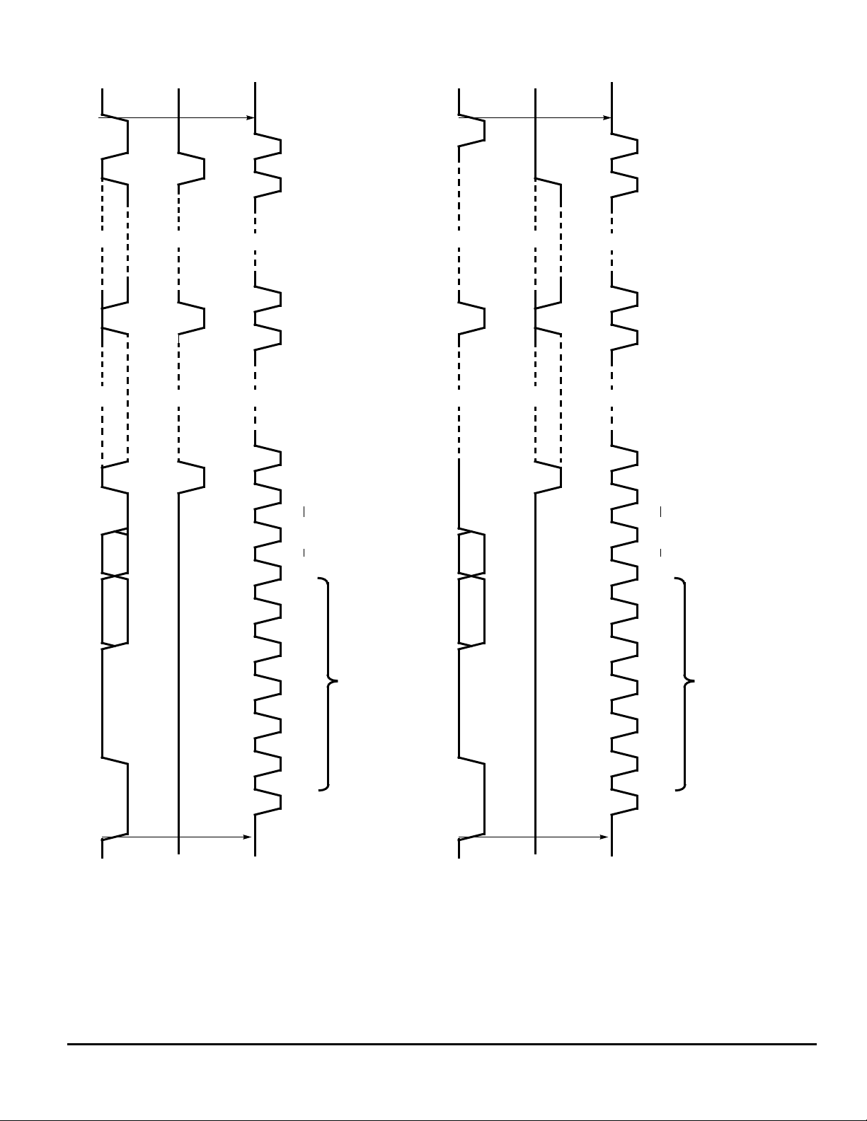
Die Pad Coordinate of MC141800A
Pad Name X(um) Y(um) Pad Name X(um) Y(um) Pad Name X(um) Y(um) Pad Name X(um) Y(um) Pad Name X(um) Y(um)
1 COM(22) -4826.0 -807.6 61 C3P 1198.4 -857.8 121 SEG(0) 4826.0 807.6 181 SEG(60) 266.0 807.6 241 SEG(120) -4294.0 807.6
2 COM(23) -4750.0 -807.6 62 C3N 1304.4 -857.8 122 SEG(1) 4750.0 807.6 182 SEG(61) 190.0 807.6 242 SEG(121) -4370.0 807.6
3 COM(24) -4674.4 -811.8 63 VLL2: 1410.4 -857.8 123 SEG(2) 4674.0 807.6 183 SEG(62) 114.0 807.6 243 SEG(122) -4446.0 807.6
4 COM(25) -4598.0 -807.6 64 VLL2: 1516.4 -857.8 124 SEG(3) 4598.0 807.6 184 SEG(63) 38.0 807.6 244 SEG(123) -4522.0 807.6
5 COM(26) -4522.0 -807.6 65 VLL3: 1622.4 -857.8 125 SEG(4) 4522.0 807.6 185 SEG(64) -38.0 807.6 245 SEG(124) -4598.0 807.6
6 COM(27) -4446.0 -807.6 66 VLL3: 1728.4 -857.8 126 SEG(5) 4446.0 807.6 186 SEG(65) -114.0 807.6 246 SEG(125) -4674.0 807.6
7 COM(28) -4370.0 -807.6 67 VLL4: 1834.4 -857.8 127 SEG(6) 4370.0 807.6 187 SEG(66) -190.0 807.6 247 SEG(126) -4750.0 807.6
8 COM(29) -4294.0 -807.6 68 VLL4: 1940.4 -857.8 128 SEG(7) 4294.0 807.6 188 SEG(67) -266.0 807.6 248 SEG(127) -4826.0 807.6
9 COM(30) -4218.0 -807.6 69 VLL5: 2046.4 -857.8 129 SEG(8) 4218.0 807.6 189 SEG(68) -342.0 807.6 249 COM64B -5328.4 835.4
10 COM(31) -4142.0 -807.6 70 VLL5: 2152.4 -857.8 130 SEG(9) 4142.0 807.6 190 SEG(69) -418.0 807.6 250 COM(0) -5328.4 759.4
11 DVDD: -4042.2 -857.8 71 VLL6: 2258.4 -857.8 131 SEG(10) 4066.0 807.6 191 SEG(70) -494.0 807.6 251 COM(1) -5328.4 683.4
12 S/P -3940.6 -857.8 72 VLL6: 2364.4 -857.8 132 SEG(11) 3990.0 807.6 192 SEG(71) -570.0 807.6 252 COM(2) -5328.4 607.4
13 RES -3839.0 -857.8 73 DVSS: 2470.4 -857.8 133 SEG(12) 3914.0 807.6 193 SEG(72) -646.0 807.6 253 COM(3) -5328.4 531.4
14 D/C -3737.4 -857.8 74 OSC1 2576.4 -857.8 134 SEG(13) 3838.0 807.6 194 SEG(73) -722.0 807.6 254 COM(4) -5328.4 455.4
15 DVSS: -3569.0 -857.8 75 DVSS: 2682.4 -857.8 135 SEG(14) 3762.0 807.6 195 SEG(74) -798.0 807.6 255 COM(5) -5328.4 379.4
16 DVSS: -3467.4 -857.8 76 DVSS: 2788.4 -857.8 136 SEG(15) 3686.0 807.6 196 SEG(75) -874.0 807.6 256 COM(6) -5328.4 303.4
17 DVSS: -3365.8 -857.8 77 VCC: 2894.4 -857.8 137 SEG(16) 3610.0 807.6 197 SEG(76) -950.0 807.6 257 COM(7) -5328.4 227.4
18 DVSS: -3264.2 -857.8 78 VCC: 3000.4 -857.8 138 SEG(17) 3534.0 807.6 198 SEG(77) -1026.0 807.6 258 COM(8) -5328.4 151.4
19 DVSS: -3162.6 -857.8 79 AVSS: 3106.4 -857.8 139 SEG(18) 3458.0 807.6 199 SEG(78) -1102.0 807.6 259 COM(9) -5328.4 75.4
20 DVSS: -3061.0 -857.8 80 OSC2 3212.4 -857.8 140 SEG(19) 3382.0 807.6 200 SEG(79) -1178.0 807.6 260 COM(10) -5328.4 -0.6
21 DVSS: -2959.4 -857.8 81 AVDD: 3318.4 -857.8 141 SEG(20) 3306.0 807.6 201 SEG(80) -1254.0 807.6 261 COM(11) -5328.4 -76.6
22 DVSS: -2857.8 -857.8 82 DVSS: 3493.0 -857.8 142 SEG(21) 3230.0 807.6 202 SEG(81) -1330.0 807.6 262 COM(12) -5328.4 -152.6
23 DVSS: -2756.2 -857.8 83 DVSS: 3594.6 -857.8 143 SEG(22) 3154.0 807.6 203 SEG(82) -1406.0 807.6 263 COM(13) -5328.4 -228.6
24 DVSS: -2654.6 -857.8 84 DVSS: 3696.2 -857.8 144 SEG(23) 3078.0 807.6 204 SEG(83) -1482.0 807.6 264 COM(14) -5328.4 -304.6
25 DVSS: -2553.0 -857.8 85 DVSS: 3797.8 -857.8 145 SEG(24) 3002.0 807.6 205 SEG(84) -1558.0 807.6 265 COM(15) -5328.4 -380.6
26 DVSS: -2451.4 -857.8 86 DVSS: 3899.4 -857.8 146 SEG(25) 2926.0 807.6 206 SEG(85) -1634.0 807.6 266 COM(16) -5328.4 -456.6
27 DVSS: -2349.8 -857.8 87 DVSS: 4001.0 -857.8 147 SEG(26) 2850.0 807.6 207 SEG(86) -1710.0 807.6 267 COM(17) -5328.4 -532.6
28 DVSS: -2248.2 -857.8 88 COM64A 4142.0 -807.6 148 SEG(27) 2774.0 807.6 208 SEG(87) -1786.0 807.6 268 COM(18) -5328.4 -608.6
29 DVSS: -2146.6 -857.8 89 COM(63) 4217.0 -806.2 149 SEG(28) 2698.0 807.6 209 SEG(88) -1862.0 807.6 269 COM(19) -5328.4 -684.6
30 DVSS: -2045.0 -857.8 90 COM(62) 4293.0 -806.2 150 SEG(29) 2622.0 807.6 210 SEG(89) -1938.0 807.6 270 COM(20) -5328.4 -760.6
31 DVSS: -1943.4 -857.8 91 COM(61) 4369.0 -806.2 151 SEG(30) 2546.0 807.6 211 SEG(90) -2014.0 807.6 271 COM(21) -5328.4 -836.6
32 DVSS: -1841.8 -857.8 92 COM(60) 4445.0 -806.2 152 SEG(31) 2470.0 807.6 212 SEG(91) -2090.0 807.6
33 DVSS: -1740.2 -857.8 93 COM(59) 4521.0 -806.2 153 SEG(32) 2394.0 807.6 213 SEG(92) -2166.0 807.6
34 R/W -1638.6 -857.8 94 COM(58) 4597.0 -806.2 154 SEG(33) 2318.0 807.6 214 SEG(93) -2242.0 807.6
35 D7 -1537.0 -857.8 95 COM(57) 4673.0 -806.2 155 SEG(34) 2242.0 807.6 215 SEG(94) -2318.0 807.6
36 D6 -1435.4 -857.8 96 COM(56) 4749.0 -806.2 156 SEG(35) 2166.0 807.6 216 SEG(95) -2394.0 807.6
37 D5 -1333.8 -857.8 97 COM(55) 4826.0 -807.6 157 SEG(36) 2090.0 807.6 217 SEG(96) -2470.0 807.6
38 D4 -1232.2 -857.8 98 COM(54) 5328.4 -836.6 158 SEG(37) 2014.0 807.6 218 SEG(97) -2546.0 807.6
39 D3 -1130.6 -857.8 99 COM(53) 5328.4 -760.6 159 SEG(38) 1938.0 807.6 219 SEG(98) -2622.0 807.6
40 D2 -1029.0 -857.8 100 COM(52) 5328.4 -684.6 160 SEG(39) 1862.0 807.6 220 SEG(99) -2698.0 807.6
41 D1 -927.4 -857.8 101 COM(51) 5328.4 -608.6 161 SEG(40) 1786.0 807.6 221 SEG(100) -2774.0 807.6
42 D0 -825.8 -857.8 102 COM(50) 5328.4 -532.6 162 SEG(41) 1710.0 807.6 222 SEG(101) -2850.0 807.6
43 D0 -724.2 -857.8 103 COM(49) 5328.4 -456.6 163 SEG(42) 1634.0 807.6 223 SEG(102) -2926.0 807.6
44 CLK -622.6 -857.8 104 COM(48) 5328.4 -380.6 164 SEG(43) 1558.0 807.6 224 SEG(103) -3002.0 807.6
45 CLK -521.0 -857.8 105 COM(47) 5328.4 -304.6 165 SEG(44) 1482.0 807.6 225 SEG(104) -3078.0 807.6
46 CE -419.6 -857.8 106 COM(46) 5328.4 -228.6 166 SEG(45) 1406.0 807.6 226 SEG(105) -3154.0 807.6
47 DVDD: -317.8 -857.8 107 COM(45) 5328.4 -152.6 167 SEG(46) 1330.0 807.6 227 SEG(106) -3230.0 807.6
48 DVDD: -216.2 -857.8 108 COM(44) 5328.4 -76.6 168 SEG(47) 1254.0 807.6 228 SEG(107) -3306.0 807.6
49 DVSS: -114.6 -857.8 109 COM(43) 5328.4 -0.6 169 SEG(48) 1178.0 807.6 229 SEG(108) -3382.0 807.6
50 DVSS: -13.0 -857.8 110 COM(42) 5328.4 75.4 170 SEG(49) 1102.0 807.6 230 SEG(109) -3458.0 807.6
51 AVDD: 138.4 -857.8 111 COM(41) 5328.4 151.4 171 SEG(50) 1026.0 807.6 231 SEG(110) -3534.0 807.6
52 AVDD: 244.4 -857.8 112 COM(40) 5328.4 227.4 172 SEG(51) 950.0 807.6 232 SEG(111) -3610.0 807.6
53 AVSS: 350.4 -857.8 113 COM(39) 5328.4 303.4 173 SEG(52) 874.0 807.6 233 SEG(112) -3686.0 807.6
54 AVSS: 456.4 -857.8 114 COM(38) 5328.4 379.4 174 SEG(53) 798.0 807.6 234 SEG(113) -3762.0 807.6
55 VF 562.4 -857.8 115 COM(37) 5328.4 455.4 175 SEG(54) 722.0 807.6 235 SEG(114) -3838.0 807.6
56 VR 668.4 -857.8 116 COM(36) 5328.4 531.4 176 SEG(55) 646.0 807.6 236 SEG(115) -3914.0 807.6
57 C1P 774.4 -857.8 117 COM(35) 5328.4 607.4 177 SEG(56) 570.0 807.6 237 SEG(116) -3990.0 807.6
58 C1N 880.4 -857.8 118 COM(34) 5328.4 683.4 178 SEG(57) 494.0 807.6 238 SEG(117) -4066.0 807.6
59 C2P 986.4 -857.8 119 COM(33) 5328.4 759.4 179 SEG(58) 418.0 807.6 239 SEG(118) -4142.0 807.6
60 C2N 1092.4 -857.8 120 COM(32) 5328.4 835.4 180 SEG(59) 342.0 807.6 240 SEG(119) -4218.0 807.6
Note : *Power and ground die pads should be bonded correspondingly in COG application
Die Pad 15 - 33, 43, 45, 47 -54, 64, 66, 68, 70, 72 - 73, 76, 78 and 82 - 87 are multiple pads of critical signal
(Basically, these are D0, CLK, DVDD, DVSS, AVDD, AVSS, VCC and VLL2-VLL6 which special design for COG)
Bump Size : Pad X(um) Y(um) Die Size (including scribe) : 11226.8 x 2286 (um)
1-10 42 100
11-87 65 65
88-97 42 100
98-120 100 42
121-248 42 100
249-271 100 42
MC141800A
3–308
MOTOROLA
 Loading...