

MOTOROLA MC14099BDWR2, MC14099BF, MC14099BFEL, MC14099BFL1, MC14099BCP Datasheet
...
Semiconductor Components Industries, LLC, 2000
March, 2000 – Rev. 3
1 Publication Order Number:
MC14099B/D
MC14099B
8-Bit Addressable Latches
The MC14099B is an 8–bit addressable latch. Data is entered in
serial form when the appropriate latch is addressed (via address pins
A0, A1, A2) and write disable is in the low state. For the MC14099B
the input is a unidirectional write only port.
The data is presented in parallel at the output of the eight latches
independently of the state of Write Disable, Write/Read
or Chip
Enable.
A Master Reset capability is available on both parts.
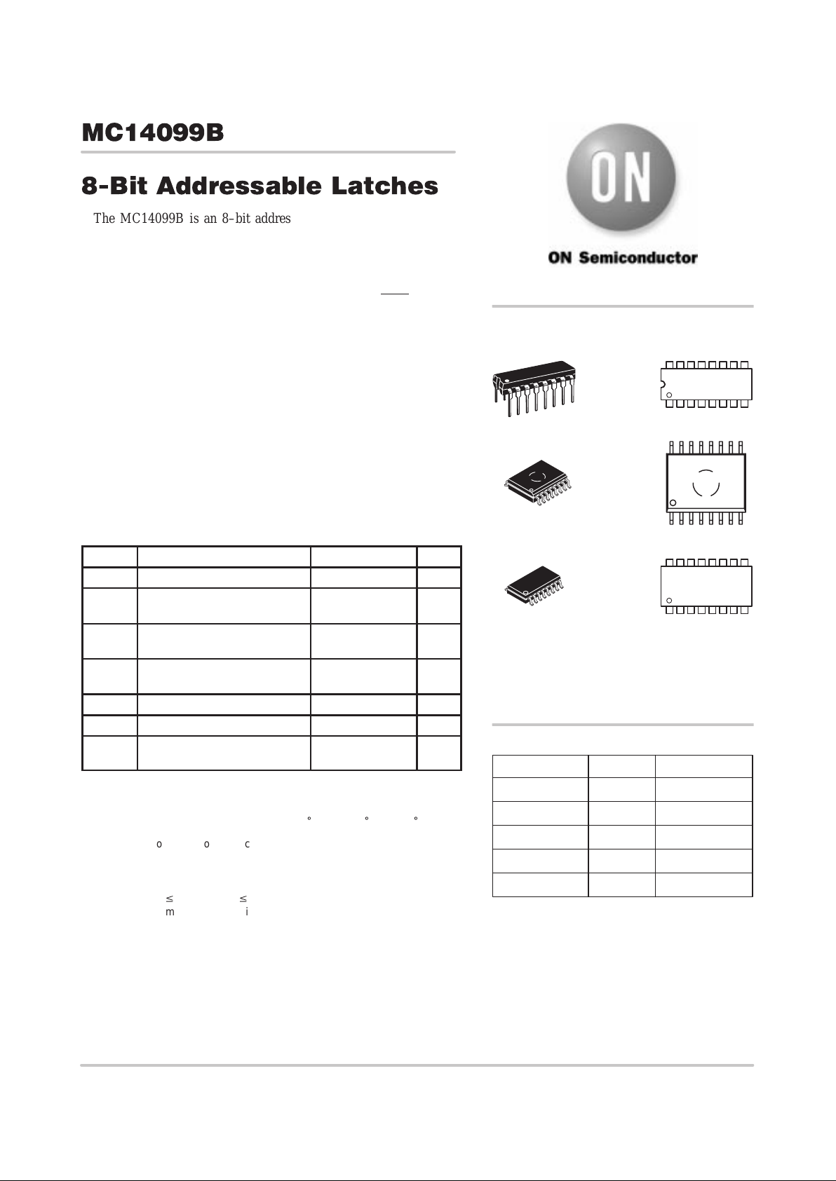
• Serial Data Input
• Parallel Output
• Master Reset
• Supply Voltage Range = 3.0 Vdc to 18 Vdc
• Capable of Driving Two Low–power TTL Loads or One Low–Power
Schottky TTL Load over the Rated Temperature Range
• MC14099B pin for pin compatible with CD4099B
MAXIMUM RATINGS (Voltages Referenced to V
SS
) (Note 2.)
Symbol Parameter Value Unit
V
DD
DC Supply Voltage Range –0.5 to +18.0 V
Vin, V
out
Input or Output Voltage Range
(DC or Transient)
–0.5 to VDD + 0.5 V
Iin, I
out
Input or Output Current
(DC or Transient) per Pin
±10 mA
P
D
Power Dissipation,
per Package (Note 3.)
500 mW
T
A
Ambient Temperature Range –55 to +125 °C
T
stg
Storage Temperature Range –65 to +150 °C
T
L
Lead Temperature
(8–Second Soldering)
260 °C
2. Maximum Ratings are those values beyond which damage to the device
may occur.
3. Temperature Derating:
Plastic “P and D/DW” Packages: – 7.0 mW/_C From 65_C T o 125_C
This device contains protection circuitry to guard against damage due to high
static voltages or electric fields. However, precautions must be taken to avoid
applications of any voltage higher than maximum rated voltages to this
high–impedance circuit. For proper operation, V
in
and V
out
should be constrained
to the range V
SS
v (Vin or V
out
) v VDD.
Unused inputs must always be tied to an appropriate logic voltage level (e.g.,
either V
SS
or VDD). Unused outputs must be left open.
Device Package Shipping
ORDERING INFORMATION
MC14099BCP PDIP–16 2000/Box
MC14099BDW SOIC–16
http://onsemi.com
2350/Box
MC14099BDWR2 SOIC–16 1000/Tape & Reel
MC14099BF SOEIAJ–16 See Note 1.
MC14099BFEL SOEIAJ–16
See Note 1.
MARKING
DIAGRAMS
1
16
PDIP–16
P SUFFIX
CASE 648
MC14099BCP
AWLYYWW
A = Assembly Location
WL or L = Wafer Lot
YY or Y = Year
WW or W = Work Week
SOEIAJ–16
F SUFFIX
CASE 966
1
16
MC14099B
AWLYWW
1. For ordering information on the EIAJ version of
the SOIC packages, please contact your local
ON Semiconductor representative.
SOIC–16
DW SUFFIX
CASE 751G
1
16
14099B
AWLYYWW
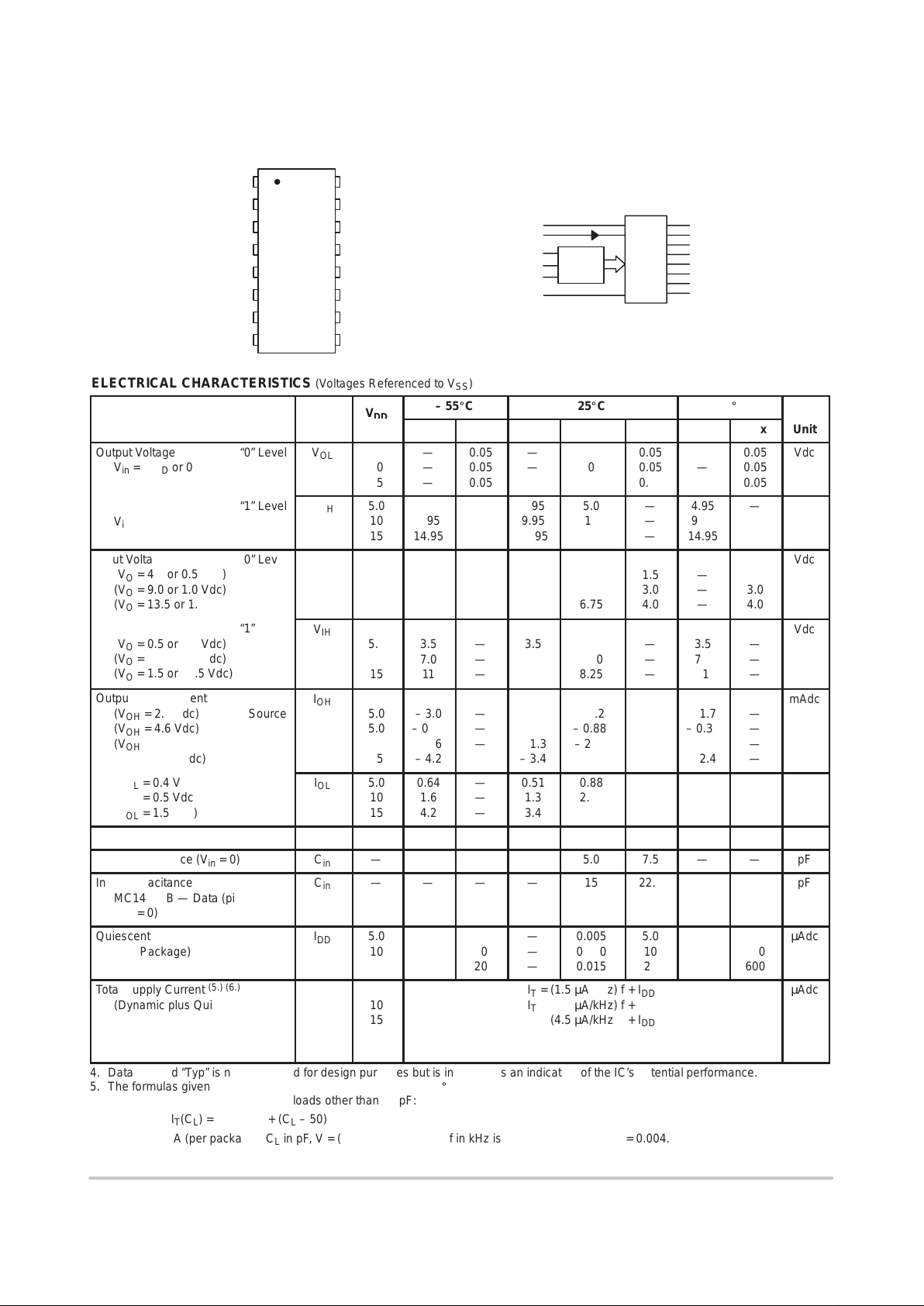
MC14099B
http://onsemi.com
2
MC14099B
13
14
15
16
9
10
11
125
4
3
2
1
8
7
6
Q3
Q4
Q5
Q6
V
DD
Q0
Q1
Q2
WRITE
DISABLE
DATA
RESET
Q7
V
SS
A2
A1
A0
PIN ASSIGNMENT
Q7
Q6
Q5
Q4
Q3
Q2
Q1
Q0
8
LATCHES
DECODER
5
6
7
WRITE DISABLE
DATA
A0
A1
A2
RESET
4
3
2
8
V
DD
= 16
V
SS
= 8
9
10
11
12
13
14
15
1
ELECTRICAL CHARACTERISTICS (Voltages Referenced to V
SS
)
V
– 55_C
25_C
125_C
Characteristic
Symbol
V
DD
Vdc
Min
Max
Min
Typ
(4.)
Max
Min
Max
Unit
ОООООООО
Î
ОООООООО
Î
Output Voltage “0” Level
V
in
= VDD or 0
ÎÎ
Î
ÎÎ
Î
V
OL
Î
Î
Î
Î
5.0
10
15
Î
Î
Î
Î
—
—
—
Î
Î
Î
Î
0.05
0.05
0.05
ÎÎ
Î
ÎÎ
Î
—
—
—
Î
Î
Î
Î
0
0
0
ÎÎ
Î
ÎÎ
Î
0.05
0.05
0.05
Î
Î
Î
Î
—
—
—
Î
Î
Î
Î
0.05
0.05
0.05
Î
Î
Î
Î
Vdc
ОООООООО
Î
“1” Level
V
in
= 0 or V
DD
ÎÎ
Î
V
OH
Î
Î
5.0
10
15
Î
Î
4.95
9.95
14.95
Î
Î
—
—
—
ÎÎ
Î
4.95
9.95
14.95
Î
Î
5.0
10
15
ÎÎ
Î
—
—
—
Î
Î
4.95
9.95
14.95
Î
Î
—
—
—
Î
Î
Vdc
ОООООООО
Î
ОООООООО
Î
Input Voltage “0” Level
(V
O
= 4.5 or 0.5 Vdc)
(V
O
= 9.0 or 1.0 Vdc)
(V
O
= 13.5 or 1.5 Vdc)
ÎÎ
Î
ÎÎ
Î
V
IL
Î
Î
Î
Î
5.0
10
15
Î
Î
Î
Î
—
—
—
Î
Î
Î
Î
1.5
3.0
4.0
ÎÎ
Î
ÎÎ
Î
—
—
—
Î
Î
Î
Î
2.25
4.50
6.75
ÎÎ
Î
ÎÎ
Î
1.5
3.0
4.0
Î
Î
Î
Î
—
—
—
Î
Î
Î
Î
1.5
3.0
4.0
Î
Î
Î
Î
Vdc
ОООООООО
Î
ОООООООО
Î
“1” Level
(V
O
= 0.5 or 4.5 Vdc)
(V
O
= 1.0 or 9.0 Vdc)
(V
O
= 1.5 or 13.5 Vdc)
ÎÎ
Î
ÎÎ
Î
V
IH
Î
Î
Î
Î
5.0
10
15
Î
Î
Î
Î
3.5
7.0
11
Î
Î
Î
Î
—
—
—
ÎÎ
Î
ÎÎ
Î
3.5
7.0
11
Î
Î
Î
Î
2.75
5.50
8.25
ÎÎ
Î
ÎÎ
Î
—
—
—
Î
Î
Î
Î
3.5
7.0
11
Î
Î
Î
Î
—
—
—
Î
Î
Î
Î
Vdc
ОООООООО
Î
ОООООООО
Î
Output Drive Current
(V
OH
= 2.5 Vdc) Source
(V
OH
= 4.6 Vdc)
(V
OH
= 9.5 Vdc)
(V
OH
= 13.5 Vdc)
ÎÎ
Î
ÎÎ
Î
I
OH
Î
Î
Î
Î
5.0
5.0
10
15
Î
Î
Î
Î
– 3.0
– 0.64
– 1.6
– 4.2
Î
Î
Î
Î
—
—
—
—
ÎÎ
Î
ÎÎ
Î
– 2.4
– 0.51
– 1.3
– 3.4
Î
Î
Î
Î
– 4.2
– 0.88
– 2.25
– 8.8
ÎÎ
Î
ÎÎ
Î
—
—
—
—
Î
Î
Î
Î
– 1.7
– 0.36
– 0.9
– 2.4
Î
Î
Î
Î
—
—
—
—
Î
Î
Î
Î
mAdc
ОООООООО
Î
ОООООООО
Î
(VOL = 0.4 Vdc) Sink
(V
OL
= 0.5 Vdc)
(V
OL
= 1.5 Vdc)
ÎÎ
Î
ÎÎ
Î
I
OL
Î
Î
Î
Î
5.0
10
15
Î
Î
Î
Î
0.64
1.6
4.2
Î
Î
Î
Î
—
—
—
ÎÎ
Î
ÎÎ
Î
0.51
1.3
3.4
Î
Î
Î
Î
0.88
2.25
8.8
ÎÎ
Î
ÎÎ
Î
—
—
—
Î
Î
Î
Î
0.36
0.9
2.4
Î
Î
Î
Î
—
—
—
Î
Î
Î
Î
mAdc
Input Current
I
in
15
—
± 0.1
—
±0.00001
± 0.1
—
± 1.0
µAdc
Input Capacitance (Vin = 0)
C
in
—
—
—
—
5.0
7.5
—
—
pF
ОООООООО
Î
Input Capacitance
MC14599B — Data (pin 3)
(V
in
= 0)
ÎÎ
Î
C
in
Î
Î
—
Î
Î
—
Î
Î
—
ÎÎ
Î
—
Î
Î
15
ÎÎ
Î
22.5
Î
Î
—
Î
Î
—
Î
Î
pF
ОООООООО
Î
Quiescent Current
(Per Package)
ÎÎ
Î
I
DD
Î
Î
5.0
10
15
Î
Î
—
—
—
Î
Î
5.0
10
20
ÎÎ
Î
—
—
—
Î
Î
0.005
0.010
0.015
ÎÎ
Î
5.0
10
20
Î
Î
—
—
—
Î
Î
150
300
600
Î
Î
µAdc
ОООООООО
Î
ОООООООО
Î
ОООООООО
Î
Total Supply Current
(5.) (6.)
(Dynamic plus Quiescent,
Per Package)
(C
L
= 50 pF on all outputs, all
buffers switching)
ÎÎ
Î
ÎÎ
Î
ÎÎ
Î
I
T
Î
Î
Î
Î
Î
Î
5.0
10
15
ООООООООООООООО
Î
ООООООООООООООО
Î
ООООООООООООООО
Î
IT = (1.5 µA/kHz) f + I
DD
IT = (3.0 µA/kHz) f + I
DD
IT = (4.5 µA/kHz) f + I
DD
Î
Î
Î
Î
Î
Î
µAdc
4. Data labelled “Typ” is not to be used for design purposes but is intended as an indication of the IC’s potential performance.
5. The formulas given are for the typical characteristics only at 25_C.
6. To calculate total supply current at loads other than 50 pF:
I
T(CL
) = IT(50 pF) + (CL – 50) Vfk
where: I
T
is in µA (per package), CL in pF, V = (VDD – VSS) in volts, f in kHz is input frequency, and k = 0.004.
MC14099B
http://onsemi.com
3
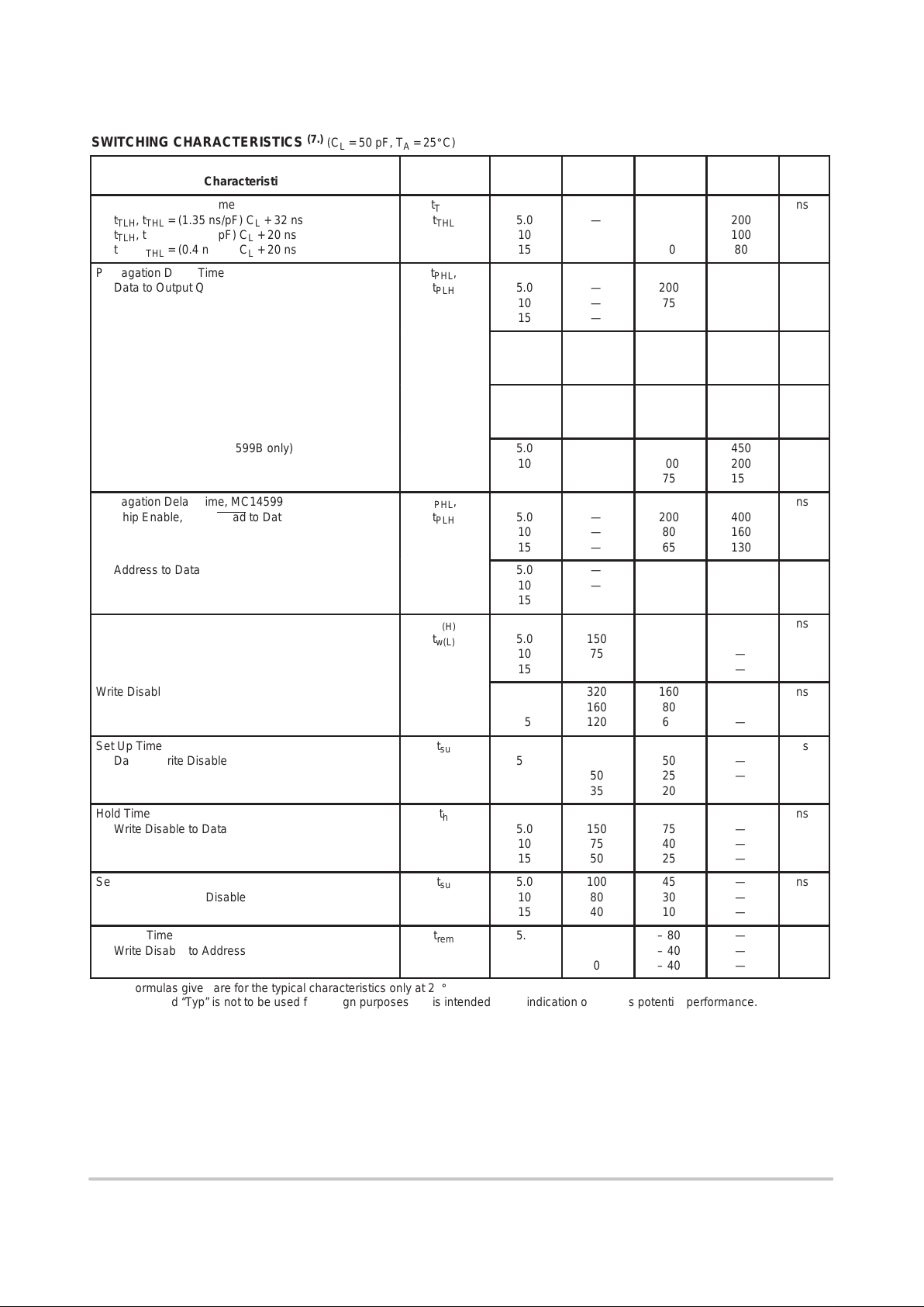
SWITCHING CHARACTERISTICS
(7.)
(C
L
= 50 pF, T
A
= 25_C)
ООООООООООООО
Î
Characteristic
ÎÎÎ
Î
Symbol
ÎÎ
Î
V
DD
Vdc
ÎÎ
Î
Min
ÎÎ
Î
Typ
(8.)
ÎÎ
Î
Max
Î
Î
Unit
ООООООООООООО
Î
Output Rise and Fall Time
t
TLH
, t
THL
= (1.35 ns/pF) CL + 32 ns
t
TLH
, t
THL
= (0.6 ns/pF) CL + 20 ns
t
TLH
, t
THL
= (0.4 ns/pF) CL + 20 ns
ÎÎÎ
Î
t
TLH
,
t
THL
ÎÎ
Î
5.0
10
15
ÎÎ
Î
—
—
—
ÎÎ
Î
100
50
40
ÎÎ
Î
200
100
80
Î
Î
ns
ООООООООООООО
Î
ООООООООООООО
Î
Propagation Delay Time
Data to Output Q
ÎÎÎ
Î
ÎÎÎ
Î
t
PHL
,
t
PLH
ÎÎ
Î
ÎÎ
Î
5.0
10
15
ÎÎ
Î
ÎÎ
Î
—
—
—
ÎÎ
Î
ÎÎ
Î
200
75
50
ÎÎ
Î
ÎÎ
Î
400
150
100
Î
Î
Î
Î
ns
ООООООООООООО
Î
ООООООООООООО
Î
Write Disable to Output Q
ÎÎÎ
Î
ÎÎÎ
Î
ÎÎ
Î
ÎÎ
Î
5.0
10
15
ÎÎ
Î
ÎÎ
Î
—
—
—
ÎÎ
Î
ÎÎ
Î
200
80
60
ÎÎ
Î
ÎÎ
Î
400
160
120
Î
Î
Î
Î
ns
ООООООООООООО
Î
Reset to Output Q
ÎÎÎÎÎÎ
Î
5.0
10
15
ÎÎ
Î
—
—
—
ÎÎ
Î
175
80
65
ÎÎ
Î
350
160
130
Î
Î
ns
ООООООООООООО
Î
CE to Output Q (MC14599B only)
ÎÎÎÎÎÎ
Î
5.0
10
15
ÎÎ
Î
—
—
—
ÎÎ
Î
225
100
75
ÎÎ
Î
450
200
150
Î
Î
ns
ООООООООООООО
Î
ООООООООООООО
Î
Propagation Delay Time, MC14599B only
Chip Enable, Write/Read
to Data
ÎÎÎ
Î
ÎÎÎ
Î
t
PHL
,
t
PLH
ÎÎ
Î
ÎÎ
Î
5.0
10
15
ÎÎ
Î
ÎÎ
Î
—
—
—
ÎÎ
Î
ÎÎ
Î
200
80
65
ÎÎ
Î
ÎÎ
Î
400
160
130
Î
Î
Î
Î
ns
ООООООООООООО
Î
ООООООООООООО
Î
Address to Data
ÎÎÎ
Î
ÎÎÎ
Î
ÎÎ
Î
ÎÎ
Î
5.0
10
15
ÎÎ
Î
ÎÎ
Î
—
—
—
ÎÎ
Î
ÎÎ
Î
200
90
75
ÎÎ
Î
ÎÎ
Î
400
180
150
Î
Î
Î
Î
ns
ООООООООООООО
Î
ООООООООООООО
Î
Pulse Widths
Reset
ÎÎÎ
Î
ÎÎÎ
Î
t
w(H)
t
w(L)
ÎÎ
Î
ÎÎ
Î
5.0
10
15
ÎÎ
Î
ÎÎ
Î
150
75
50
ÎÎ
Î
ÎÎ
Î
75
40
25
ÎÎ
Î
ÎÎ
Î
—
—
—
Î
Î
Î
Î
ns
ООООООООООООО
Î
Write Disable
ÎÎÎÎÎÎ
Î
5.0
10
15
ÎÎ
Î
320
160
120
ÎÎ
Î
160
80
60
ÎÎ
Î
—
—
—
Î
Î
ns
ООООООООООООО
Î
ООООООООООООО
Î
Set Up Time
Data to Write Disable
ÎÎÎ
Î
ÎÎÎ
Î
t
su
ÎÎ
Î
ÎÎ
Î
5.0
10
15
ÎÎ
Î
ÎÎ
Î
100
50
35
ÎÎ
Î
ÎÎ
Î
50
25
20
ÎÎ
Î
ÎÎ
Î
—
—
—
Î
Î
Î
Î
ns
ООООООООООООО
Î
ООООООООООООО
Î
Hold Time
Write Disable to Data
ÎÎÎ
Î
ÎÎÎ
Î
t
h
ÎÎ
Î
ÎÎ
Î
5.0
10
15
ÎÎ
Î
ÎÎ
Î
150
75
50
ÎÎ
Î
ÎÎ
Î
75
40
25
ÎÎ
Î
ÎÎ
Î
—
—
—
Î
Î
Î
Î
ns
ООООООООООООО
Î
Set Up Time
Address to Write Disable
ÎÎÎ
Î
t
su
ÎÎ
Î
5.0
10
15
ÎÎ
Î
100
80
40
ÎÎ
Î
45
30
10
ÎÎ
Î
—
—
—
Î
Î
ns
ООООООООООООО
Î
Removal Time
Write Disable to Address
ÎÎÎ
Î
t
rem
ÎÎ
Î
5.0
10
15
ÎÎ
Î
0
0
0
ÎÎ
Î
– 80
– 40
– 40
ÎÎ
Î
—
—
—
Î
Î
ns
7. The formulas given are for the typical characteristics only at 25_C.
8. Data labelled “Typ” is not to be used for design purposes but is intended as an indication of the IC’s potential performance.
 Loading...