

MOTOROLA MC14093BDTR2, MC14093BF, MC14093BCP, MC14093BD, MC14093BDR2 Datasheet
...
Semiconductor Components Industries, LLC, 2000
March, 2000 – Rev. 3
1 Publication Order Number:
MC14093B/D
MC14093B
Quad 2-Input NAND"
Schmitt Trigger
The MC14093B Schmitt trigger is constructed with MOS
P–channel and N–channel enhancement mode devices in a single
monolithic structure. These devices find primary use where low power
dissipation and/or high noise immunity is desired. The MC14093B
may be used in place of the MC14011B quad 2–input NAND gate for
enhanced noise immunity or to “square up” slowly changing
waveforms.
• Supply Voltage Range = 3.0 Vdc to 18 Vdc
• Capable of Driving Two Low–Power TTL Loads or One Low–Power
Schottky TTL Load Over the Rated Temperature Range
• Triple Diode Protection on All Inputs
• Pin–for–Pin Compatible with CD4093
• Can be Used to Replace MC14011B
• Independent Schmitt–Trigger at each Input
MAXIMUM RATINGS (Voltages Referenced to V
SS
) (Note 2.)
Symbol Parameter Value Unit
V
DD
DC Supply Voltage Range –0.5 to +18.0 V
Vin, V
out
Input or Output Voltage Range
(DC or Transient)
–0.5 to VDD + 0.5 V
Iin, I
out
Input or Output Current
(DC or Transient) per Pin
±10 mA
P
D
Power Dissipation,
per Package (Note 3.)
500 mW
T
A
Ambient Temperature Range –55 to +125 °C
T
stg
Storage Temperature Range –65 to +150 °C
T
L
Lead Temperature
(8–Second Soldering)
260 °C
2. Maximum Ratings are those values beyond which damage to the device
may occur.
3. Temperature Derating:
Plastic “P and D/DW” Packages: – 7.0 mW/_C From 65_C T o 125_C
This device contains protection circuitry to guard against damage due to high
static voltages or electric fields. However, precautions must be taken to avoid
applications of any voltage higher than maximum rated voltages to this
high–impedance circuit. For proper operation, V
in
and V
out
should be constrained
to the range V
SS
v (Vin or V
out
) v VDD.
Unused inputs must always be tied to an appropriate logic voltage level (e.g.,
either V
SS
or VDD). Unused outputs must be left open.
http://onsemi.com
A = Assembly Location
WL or L = Wafer Lot
YY or Y = Year
WW or W = Work Week
Device Package Shipping
ORDERING INFORMATION
MC14093BCP PDIP–14 2000/Box
MC14093BD SOIC–14
2750/Box
MC14093BDR2 SOIC–14 2500/Tape & Reel
MC14093BDT TSSOP–14
MC14093BF SOEIAJ–14
96/Rail
See Note 1.
MARKING
DIAGRAMS
1
14
PDIP–14
P SUFFIX
CASE 646
MC14093BCP
AWLYYWW
SOIC–14
D SUFFIX
CASE 751A
TSSOP–14
DT SUFFIX
CASE 948G
1
14
14093B
AWLYWW
14
093B
ALYW
1
14
SOEIAJ–14
F SUFFIX
CASE 965
1
14
MC14093B
AWLYWW
MC14093BFEL SOEIAJ–14 See Note 1.
1. For ordering information on the EIAJ version of
the SOIC packages, please contact your local
ON Semiconductor representative.
MC14093BDTR2 TSSOP–14 2500/Tape & Reel
MC14093BDTEL TSSOP–14 2000/Tape & Reel
MC14093B
http://onsemi.com
2
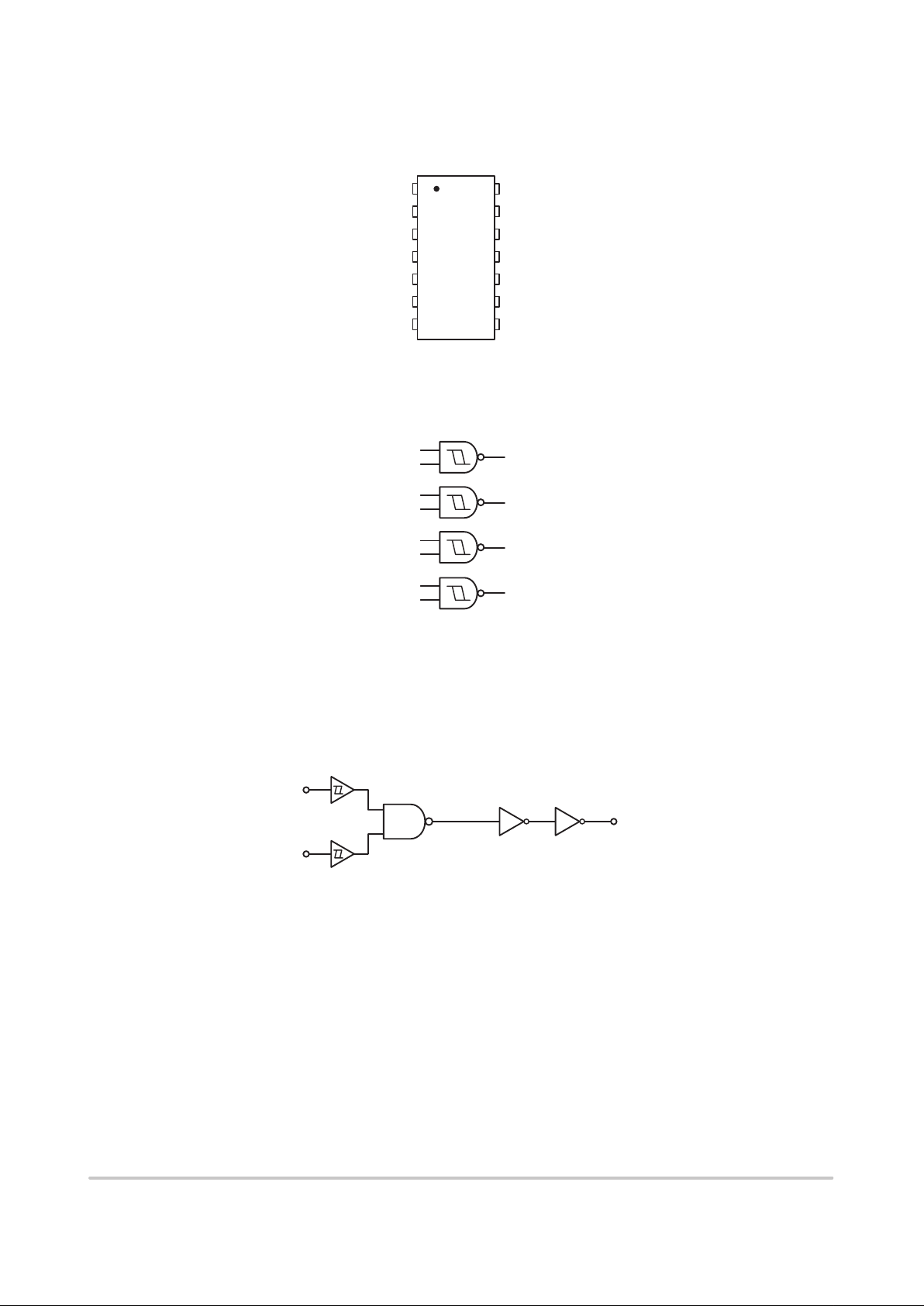
PIN ASSIGNMENT
11
12
13
14
8
9
105
4
3
2
1
7
6
OUT
C
OUT
D
IN 1
D
IN 2
D
V
DD
IN 1C
IN 2
C
OUT
B
OUT
A
IN 2
A
IN 1
A
V
SS
IN 2
B
IN 1
B
LOGIC DIAGRAM
13
11
V
DD
= PIN 14
V
SS
= PIN 7
10
4
3
12
9
8
6
5
2
1
EQUIVALENT CIRCUIT SCHEMATIC
(1/4 OF CIRCUIT SHOWN)
MC14093B
http://onsemi.com
3
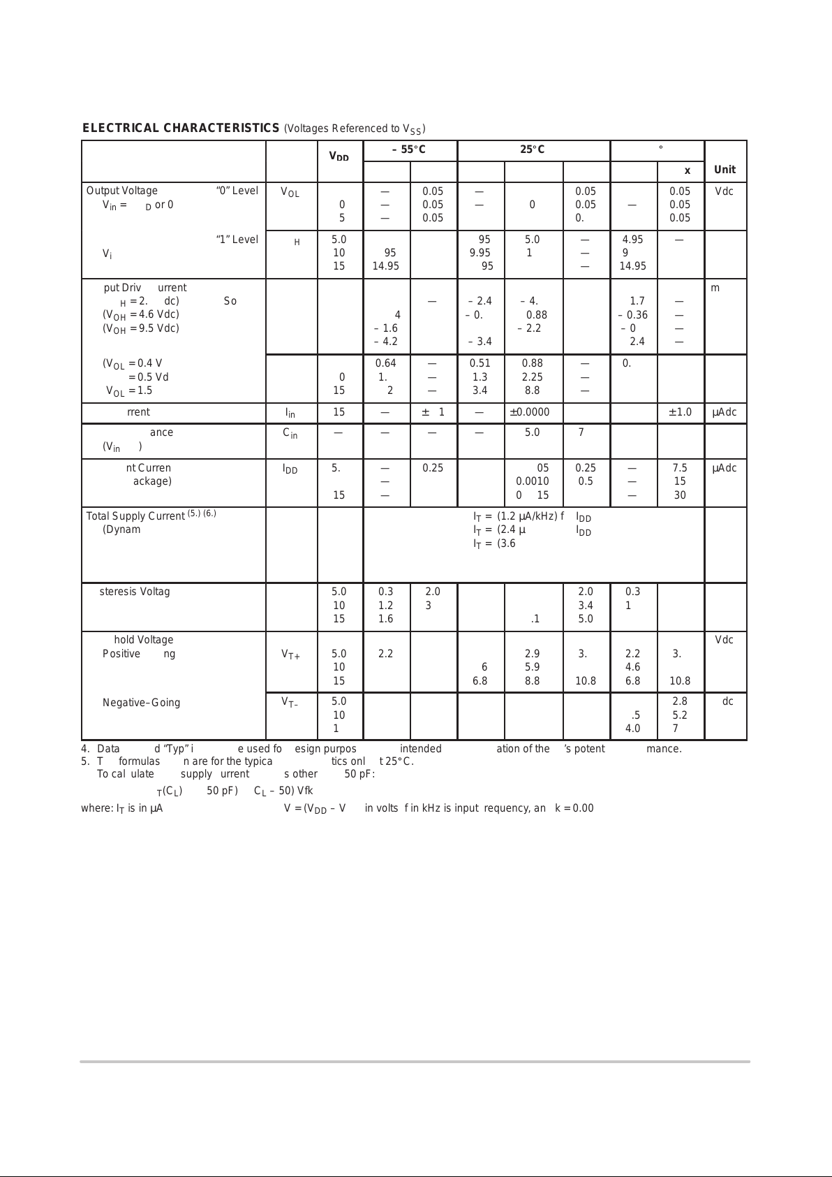
ELECTRICAL CHARACTERISTICS (Voltages Referenced to V
SS
)
V
– 55_C
25_C
125_C
Characteristic
Symbol
V
DD
Vdc
Min
Max
Min
Typ
(4.)
Max
Min
Max
Unit
ОООООООО
Î
Output Voltage “0” Level
V
in
= VDD or 0
ÎÎ
Î
V
OL
Î
Î
5.0
10
15
Î
Î
—
—
—
Î
Î
0.05
0.05
0.05
ÎÎ
Î
—
—
—
Î
Î
0
0
0
ÎÎ
Î
0.05
0.05
0.05
Î
Î
—
—
—
Î
Î
0.05
0.05
0.05
Î
Î
Vdc
ОООООООО
Î
“1” Level
V
in
= 0 or V
DD
ÎÎ
Î
V
OH
Î
Î
5.0
10
15
Î
Î
4.95
9.95
14.95
Î
Î
—
—
—
ÎÎ
Î
4.95
9.95
14.95
Î
Î
5.0
10
15
ÎÎ
Î
—
—
—
Î
Î
4.95
9.95
14.95
Î
Î
—
—
—
Î
Î
Vdc
ОООООООО
Î
ОООООООО
Î
ОООООООО
Î
Output Drive Current
(V
OH
= 2.5 Vdc) Source
(V
OH
= 4.6 Vdc)
(V
OH
= 9.5 Vdc)
(V
OH
= 13.5 Vdc)
ÎÎ
Î
ÎÎ
Î
ÎÎ
Î
I
OH
Î
Î
Î
Î
Î
Î
5.0
5.0
10
15
Î
Î
Î
Î
Î
Î
– 3.0
– 0.64
– 1.6
– 4.2
Î
Î
Î
Î
Î
Î
—
—
—
—
ÎÎ
Î
ÎÎ
Î
ÎÎ
Î
– 2.4
– 0.51
– 1.3
– 3.4
Î
Î
Î
Î
Î
Î
– 4.2
– 0.88
– 2.25
– 8.8
ÎÎ
Î
ÎÎ
Î
ÎÎ
Î
—
—
—
—
Î
Î
Î
Î
Î
Î
– 1.7
– 0.36
– 0.9
– 2.4
Î
Î
Î
Î
Î
Î
—
—
—
—
Î
Î
Î
Î
Î
Î
mAdc
ОООООООО
Î
(VOL = 0.4 Vdc) Sink
(V
OL
= 0.5 Vdc)
(V
OL
= 1.5 Vdc)
ÎÎ
Î
I
OL
Î
Î
5.0
10
15
Î
Î
0.64
1.6
4.2
Î
Î
—
—
—
ÎÎ
Î
0.51
1.3
3.4
Î
Î
0.88
2.25
8.8
ÎÎ
Î
—
—
—
Î
Î
0.36
0.9
2.4
Î
Î
—
—
—
Î
Î
mAdc
Input Current
I
in
15
—
± 0.1
—
±0.00001
± 0.1
—
± 1.0
µAdc
ОООООООО
Î
Input Capacitance
(V
in
= 0)
ÎÎ
Î
C
in
Î
Î
—
Î
Î
—
Î
Î
—
ÎÎ
Î
—
Î
Î
5.0
ÎÎ
Î
7.5
Î
Î
—
Î
Î
—
Î
Î
pF
ОООООООО
Î
Quiescent Current
(Per Package)
ÎÎ
Î
I
DD
Î
Î
5.0
10
15
Î
Î
—
—
—
Î
Î
0.25
0.5
1.0
ÎÎ
Î
—
—
—
Î
Î
0.0005
0.0010
0.0015
ÎÎ
Î
0.25
0.5
1.0
Î
Î
—
—
—
Î
Î
7.5
15
30
Î
Î
µAdc
ОООООООО
Î
ОООООООО
Î
ОООООООО
Î
Total Supply Current
(5.) (6.)
(Dynamic plus Quiescent,
Per Package)
(C
L
= 50 pF on all outputs, all
buffers switching)
ÎÎ
Î
ÎÎ
Î
ÎÎ
Î
I
T
Î
Î
Î
Î
Î
Î
5.0
10
15
ООООООООООООООО
Î
ООООООООООООООО
Î
ООООООООООООООО
Î
IT = (1.2 µA/kHz) f + I
DD
IT = (2.4 µA/kHz) f + I
DD
IT = (3.6 µA/kHz) f + I
DD
Î
Î
Î
Î
Î
Î
µAdc
ОООООООО
Î
Hysteresis Voltage
ÎÎ
Î
VH†
Î
Î
5.0
10
15
Î
Î
0.3
1.2
1.6
Î
Î
2.0
3.4
5.0
ÎÎ
Î
0.3
1.2
1.6
Î
Î
1.1
1.7
2.1
ÎÎ
Î
2.0
3.4
5.0
Î
Î
0.3
1.2
1.6
Î
Î
2.0
3.4
5.0
Î
Î
Vdc
ОООООООО
Î
ОООООООО
Î
Threshold Voltage
Positive–Going
ÎÎ
Î
ÎÎ
Î
V
T+
Î
Î
Î
Î
5.0
10
15
Î
Î
Î
Î
2.2
4.6
6.8
Î
Î
Î
Î
3.6
7.1
10.8
ÎÎ
Î
ÎÎ
Î
2.2
4.6
6.8
Î
Î
Î
Î
2.9
5.9
8.8
ÎÎ
Î
ÎÎ
Î
3.6
7.1
10.8
Î
Î
Î
Î
2.2
4.6
6.8
Î
Î
Î
Î
3.6
7.1
10.8
Î
Î
Î
Î
Vdc
ОООООООО
Î
ОООООООО
Î
Negative–Going
ÎÎ
Î
ÎÎ
Î
V
T–
Î
Î
Î
Î
5.0
10
15
Î
Î
Î
Î
0.9
2.5
4.0
Î
Î
Î
Î
2.8
5.2
7.4
ÎÎ
Î
ÎÎ
Î
0.9
2.5
4.0
Î
Î
Î
Î
1.9
3.9
5.8
ÎÎ
Î
ÎÎ
Î
2.8
5.2
7.4
Î
Î
Î
Î
0.9
2.5
4.0
Î
Î
Î
Î
2.8
5.2
7.4
Î
Î
Î
Î
Vdc
4. Data labelled “Typ” is not to be used for design purposes but is intended as an indication of the IC’s potential performance.
5. The formulas given are for the typical characteristics only at 25_C.
6. To calculate total supply current at loads other than 50 pF:
I
T(CL
) = IT(50 pF) + (CL – 50) Vfk
where: I
T
is in µA (per package), CL in pF, V = (VDD – VSS) in volts, f in kHz is input frequency, and k = 0.004.
 Loading...