

MOTOROLA MC14067BDW, MC14067BDWR2, MC14067BCP Datasheet
MC14067B
Î
Î
Î
Î
Î
Î
Analog Multiplexers /
Demultiplexers
The MC14067 multiplexer/demultiplexer is a digitally controlled
analog switch featuring low ON resistance and very low leakage
current. This device can be used in either digital or analog
applications.
The MC14067 is a 16–channel multiplexer/demultiplexer with an
inhibit and four binary control inputs A, B, C, and D. These control
inputs select 1–of–16 channels by turning ON the appropriate analog
switch (see MC14067 truth table.)
• Low OFF Leakage Current
• Matched Channel Resistance
• Low Quiescent Power Consumption
• Low Crosstalk Between Channels
• Wide Operating Voltage Range: 3 to 18 V
• Low Noise
• Pin for Pin Replacement for CD4067B
http://onsemi.com
24
PDIP–24
P SUFFIX
CASE 709
24
SOIC–24
DW SUFFIX
CASE 751E
MARKING
DIAGRAMS
MC14067BCP
AWLYYWW
1
14067B
AWLYYWW
1
MAXIMUM RATINGS (Voltages Referenced to V
Symbol
V
DD
Vin, V
out
DC Supply Voltage Range
Input or Output Voltage Range
Parameter
) (Note 1.)
SS
Value
– 0.5 to + 18.0
– 0.5 to VDD + 0.5
Unit
V
V
(DC or Transient)
I
in
ÎÎ
I
sw
P
D
ÎÎ
T
A
T
stg
T
L
Input Current (DC or Transient),
ОООООООО
per Control Pin
Switch Through Current
Power Dissipation,
per Package (Note 2.)
ОООООООО
Ambient Temperature Range
Storage Temperature Range
Lead Temperature
± 10
ÎÎÎÎ
± 25
500
ÎÎÎÎ
– 55 to + 125
– 65 to + 150
260
mA
mA
mW
_
_
_
C
C
C
(8–Second Soldering)
1. Maximum Ratings are those values beyond which damage to the device
may occur.
2. Temperature Derating:
Plastic “P and D/DW” Packages: – 7.0 mW/_C From 65_C To 125_C
This device contains protection circuitry to guard against damage due to high
static voltages or electric fields. However, precautions must be taken to avoid
applications of any voltage higher than maximum rated voltages to this
high–impedance circuit. For proper operation, V
to the range V
v (Vin or V
SS
) v VDD.
out
and V
in
should be constrained
out
Unused inputs must always be tied to an appropriate logic voltage level (e.g.,
either V
or VDD). Unused outputs must be left open.
SS
A = Assembly Location
WL or L = Wafer Lot
YY or Y = Year
WW or W = Work Week
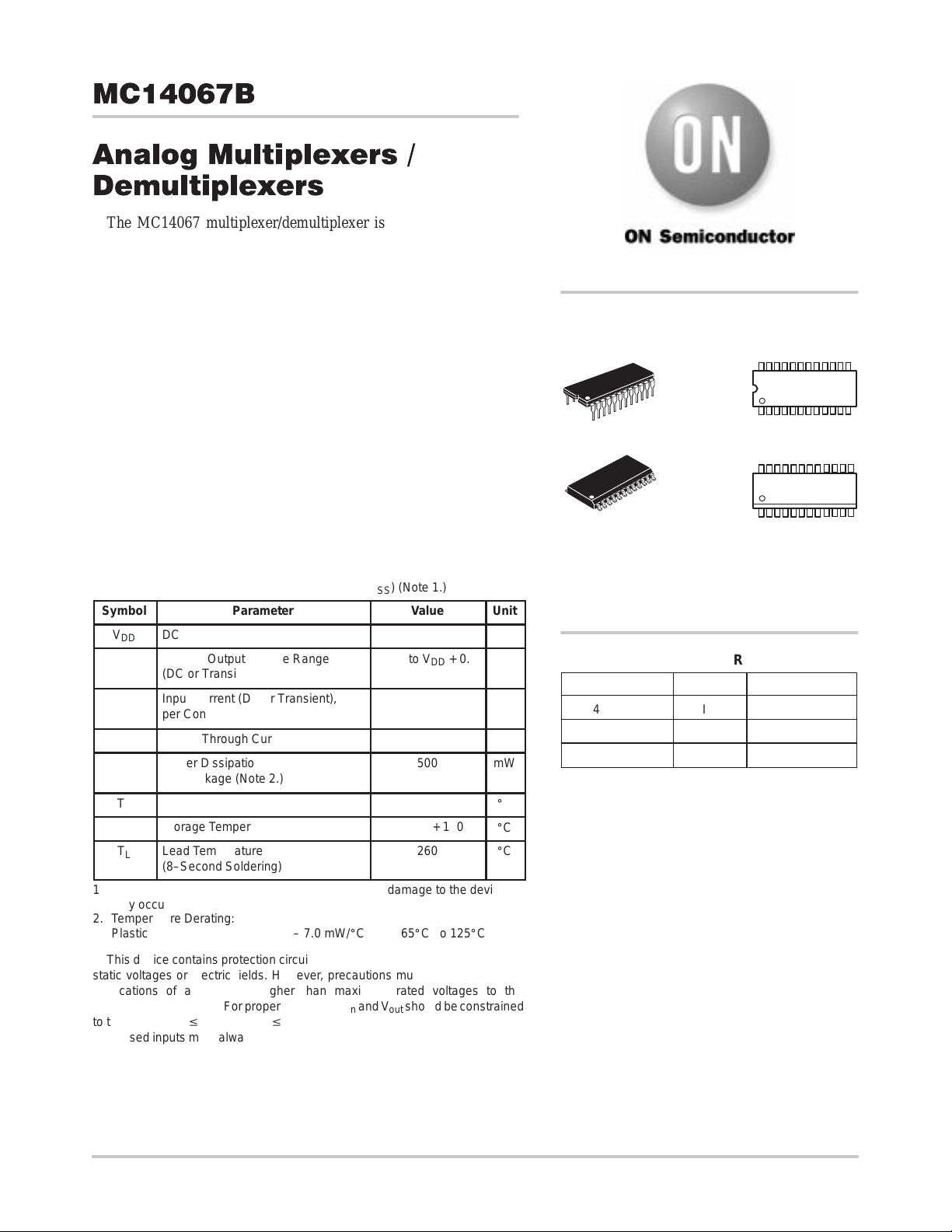
ORDERING INFORMATION
Device Package Shipping
MC14067BCP PDIP–24 15/Rail
MC14067BDW SOIC–24
MC14067BDWR2 SOIC–24 1000/Tape & Reel
30/Rail
Semiconductor Components Industries, LLC, 2000
March, 2000 – Rev . 3
1 Publication Order Number:
MC14067B/D
MC14067B
Selected
MC14067 TRUTH TABLE
Control Inputs
A B C D Inh
X X X X 1 None
0 0 0 0 0 X0
1 0 0 0 0 X1
0 1 0 0 0 X2
1 1 0 0 0 X3
0 0 1 0 0 X4
1 0 1 0 0 X5
0 1 1 0 0 X6
1 1 1 0 0 X7
0 0 0 1 0 X8
1 0 0 1 0 X9
0 1 0 1 0 X10
1 1 0 1 0 X11
0 0 1 1 0 X12
1 0 1 1 0 X13
0 1 1 1 0 X14
1 1 1 1 0 X15
Selected
Channel
MC14067B
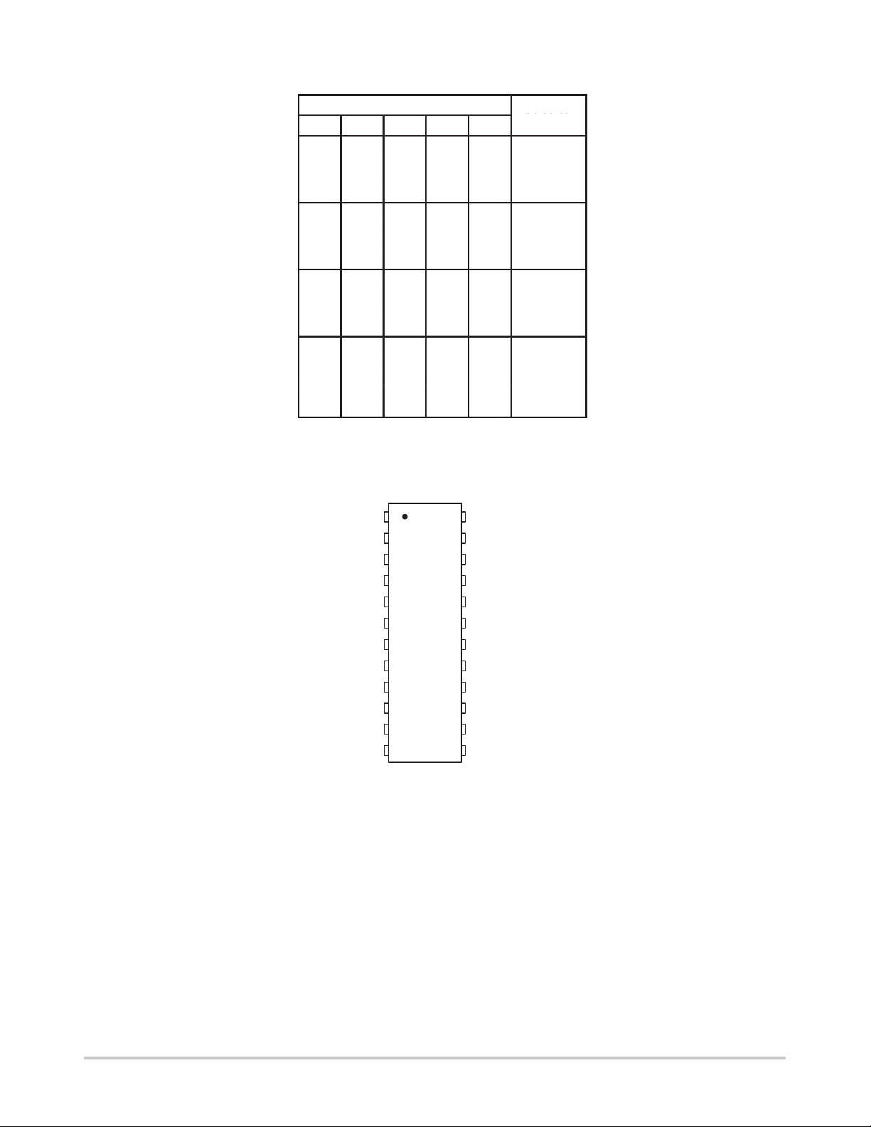
PIN ASSIGNMENT
1
X
2
X7
3
X6
4
X5
X4 X11
5
X3
6
X2
7
X1
8
9
X0
10
A
B
11
V
12
SS
24
23
22
21
20
19
18
17
16
15
14
13
V
DD
X8
X9
X10
X12
X13
X14
X15
INHIBIT
C
D
http://onsemi.com
2
CONTROLS
SWITCHES
IN/OUT
MC14067B
MC14067B
16–Channel Analog
Multiplexer/Demultiplexer
15
INHIBIT
10
A
11
B
14
C
13
D
9
X0
8
X1
7
X2
6
X3
5
X4
4
X5
3
X6
2
X7
23
X8
22
X9
21
X10
20
X11
19
X12
18
X13
17
X14
16
X15
X
COMMON
1
OUT/IN
VDD = PIN 24
V
= PIN 12
SS
CONTROL
INPUTS
X
IN/OUT
MC14067 FUNCTIONAL DIAGRAM
INHIBIT
A
X0
X1
X2
X3
X4
X5
X6
X7
X8
X9
X10
X11
X12
X13
X14
X15
B
C
D
1–OF–16 DECODER
X
OUT/IN
http://onsemi.com
3
MC14067B
Î
Î
Î
Î
Î
Î
Î
Î
Î
Î
Î
Î
Î
Î
Î
Î
Î
Î
Î
Î
Î
Î
Î
Î
Î
Î
Î
Î
Î
Î
Î
Î
Î
Î
Î
Î
Î
Î
Î
Î
Î
Î
Î
Î
Î
Î
Î
Î
Î
Î
Î
Î
Î
Î
Î
Î
Î
Î
Î
Î
Î
Î
Î
Î
Î
Î
Î
Î
Î
Î
Î
Î
Î
Î
Î
Î
Î
Î
Î
Î
Î
Î
Î
Î
Î
Î
Î
Î
Î
Î
Î
Î
Î
Î
Î
Î
Î
Î
Î
Î
Î
Î
Î
Î
Î
Î
Î
Î
Î
Î
Î
Î
Î
Î
Î
Î
Î
Î
Î
Î
Î
Î
Î
Î
Î
Î
Î
Î
Î
Î
Î
Î
Î
Î
Î
Î
Î
Î
Î
Î
Î
Î
Î
Î
Î
Î
Î
Î
Î
Î
Î
Î
Î
Î
Î
Î
Î
Î
Î
Î
Î
Î
Î
Î
Î
Î
Î
Î
Î
Î
Î
Î
Î
Î
Î
Î
Î
Î
Î
Î
Î
Î
Î
Î
Î
Î
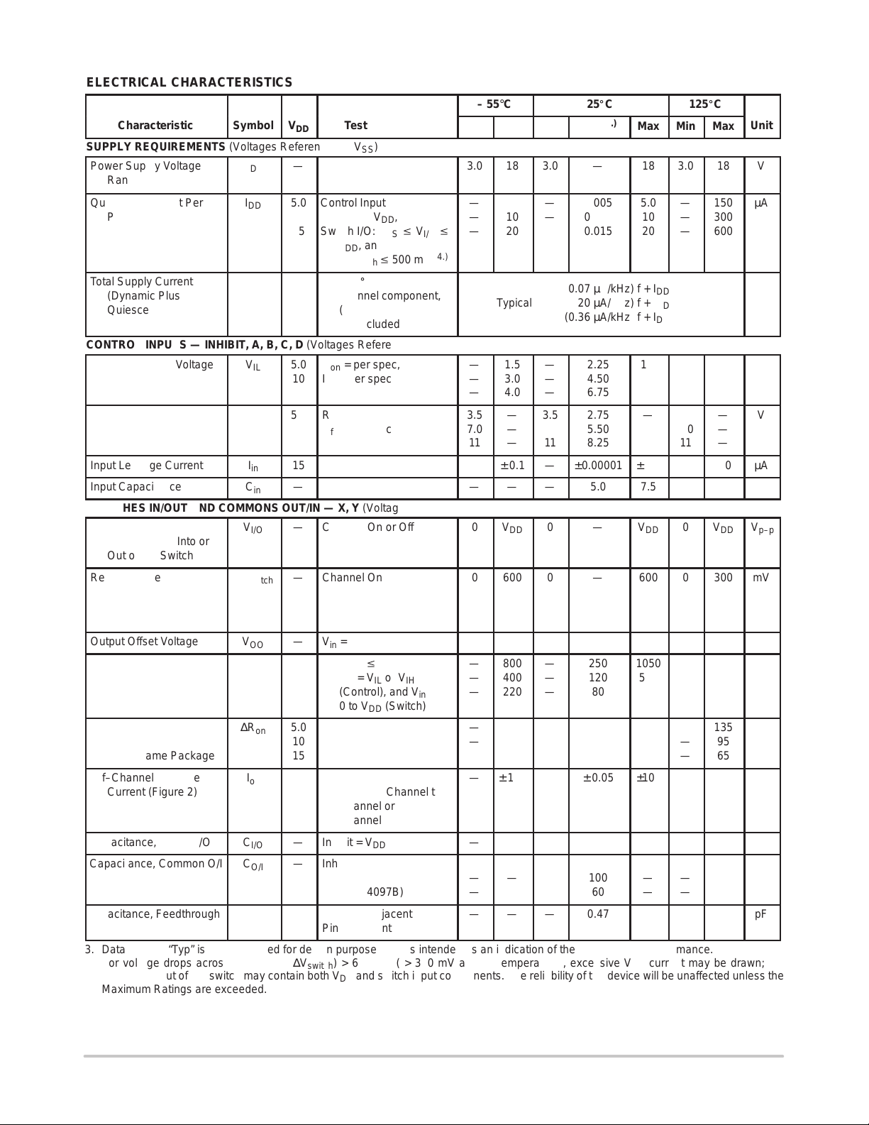
ELECTRICAL CHARACTERISTICS
– 55°C
Characteristic
Symbol
V
DD
Test Conditions
Min
Max
Min
SUPPLY REQUIREMENTS (Voltages Referenced to VSS)
Power Supply Voltage
V
DD
—
3.0
18
3.0
Range
Quiescent Current Per
ОООООО
Package
ОООООО
ОООООО
Total Supply Current
(Dynamic Plus
ОООООО
Quiescent,
ОООООО
Per Package
I
DD
Î
Î
Î
I
D(AV)
Î
Î
5.0
Control Inputs: V
Î
Î
Î
Î
Î
ООООО
10
Switch I/O: V
15
ООООО
ООООО
5.0
TA = 25_C only (The
10
ООООО
15
ООООО
VSS or VDD,
in =
v V
SS
V
∆V
DD
, and
switch
v
I/O
500 mV
channel component,
– V
(V
)/Ron, is
in
out
not included.)
—
Î
v
Î
(4.)
Î
ООООООООООООО
ООООООООООООО
5.0
Î
—
10
—
20
Î
Î
Typical (0.20 µA/kHz) f + I
CONTROL INPUTS — INHIBIT, A, B, C, D (Voltages Referenced to VSS)
Low–Level Input Voltage
ОООООО
High–Level Input Voltage
ОООООО
Input Leakage Current
Input Capacitance
V
Î
V
Î
I
C
5.0
10
Î
15
5.0
10
Î
Ron = per spec,
I
= per spec
off
ООООО
Ron = per spec,
I
= per spec
off
ООООО
IL
IH
15
15
—
Vin = 0 or V
DD
in
in
Î
3.5
7.0
Î
—
1.5
—
3.0
Î
—
4.0
—
3.5
—
7.0
Î
11
—
—
± 0.1
—
—
SWITCHES IN/OUT AND COMMONS OUT/IN — X, Y (Voltages Referenced to VSS)
Recommended Peak–to–
ОООООО
Peak Voltage Into or
Out of the Switch
ОООООО
Recommended Static or
Dynamic Voltage
Across the Switch
ОООООО
(4.)
∆V
V
Î
Î
switch
Î
I/O
—
Channel On or Off
Î
Î
—
Channel On
Î
ООООО
ООООО
ООООО
Î
Î
Î
0
V
DD
Î
Î
0
600
Î
(Figure 1)
Output Offset Voltage
ON Resistance
ОООООО
ОООООО
V
R
Î
Î
OO
on
—
Vin = 0 V, No Load
5.0
∆V
Î
10
15
Î
v 500 mV
switch
ООООО
V
= VIL or V
in
(Control), and V
ООООО
(4.)
IH
in
—
—
,
—
Î
Î
800
Î
—
400
—
220
Î
0 to VDD (Switch)
∆ON Resistance Between
ОООООО
Any Two Channels
in the Same Package
ОООООО
Off–Channel Leakage
Current (Figure 2)
ОООООО
ОООООО
Capacitance, Switch I/O
Capacitance, Common O/I
ОООООО
Capacitance, Feedthrough
(Channel Off)
ОООООО
∆R
Î
Î
I
Î
Î
C
C
Î
C
Î
off
I/O
O/I
I/O
5.0
on
Î
Î
Î
Î
ООООО
10
15
ООООО
15
Vin = VIL or V
(Control) Channel to
ООООО
Channel or Any One
Channel
ООООО
—
Inhibit = V
—
Inhibit = V
IH
DD
DD
(MC14067B)
Î
Î
ООООО
(MC14097B)
—
Pins Not Adjacent
—
Pins Adjacent
ООООО
Î
Î
Î
Î
Î
Î
—
70
Î
—
50
—
45
Î
—
± 100
Î
Î
—
—
—
—
Î
—
—
—
—
Î
3. Data labeled “Typ” is not to be used for design purposes, but is intended as an indication of the IC’s potential performance.
4. For voltage drops across the switch (∆V
the current out of the switch may contain both V
Maximum Ratings are exceeded. (See first page of this data sheet.)
) > 600 mV ( > 300 mV at high temperature), excessive VDD current may be drawn; i.e.
switch
and switch input components. The reliability of the device will be unaffected unless the
DD
25_C
(3.)
Typ
—
—
0.005
Î
—
—
Î
Î
Î
0.010
0.015
Î
Î
(0.07 µA/kHz) f + I
(0.36 µA/kHz) f + I
—
2.25
—
4.50
Î
—
Î
6.75
2.75
5.50
Î
11
—
—
Î
Î
Î
—
—
Î
—
—
Î
—
Î
—
—
Î
—
Î
Î
—
—
Î
—
—
Î
0
0
Î
8.25
±0.00001
5.0
—
Î
Î
—
Î
10
250
Î
120
80
Î
25
Î
10
10
Î
± 0.05
Î
Î
10
100
Î
60
0.47
Î
Max
18
5.0
Î
10
20
Î
Î
1.5
3.0
Î
4.0
—
—
Î
—
± 0.1
7.5
V
Î
Î
600
Î
—
1050
Î
500
280
Î
70
Î
50
45
Î
±100
Î
Î
—
—
Î
—
—
Î
DD
DD
DD
DD
Min
3.0
—
Î
—
—
Î
Î
—
—
Î
—
3.5
7.0
Î
11
—
—
0
Î
Î
0
Î
—
—
Î
—
—
Î
—
Î
—
—
Î
—
Î
Î
—
—
Î
—
—
Î
125_C
Max
18
150
Î
300
600
Î
Î
1.5
3.0
Î
4.0
—
—
Î
—
1.0
—
V
DDVp–p
Î
Î
300
Î
—
1300
Î
550
320
Î
135
Î
95
65
Î
±1000
Î
Î
—
—
Î
—
—
Î
Unit
V
µA
µA
V
V
µA
pF
mV
µV
Ω
Ω
nA
pF
pF
pF
http://onsemi.com
4
 Loading...