

Motorola MC14044BCL, MC14044BCP, MC14044BD, MC14043BD, MC14043BCL Datasheet
...
MOTOROLA CMOS LOGIC DATAMC14043B MC14044B
162
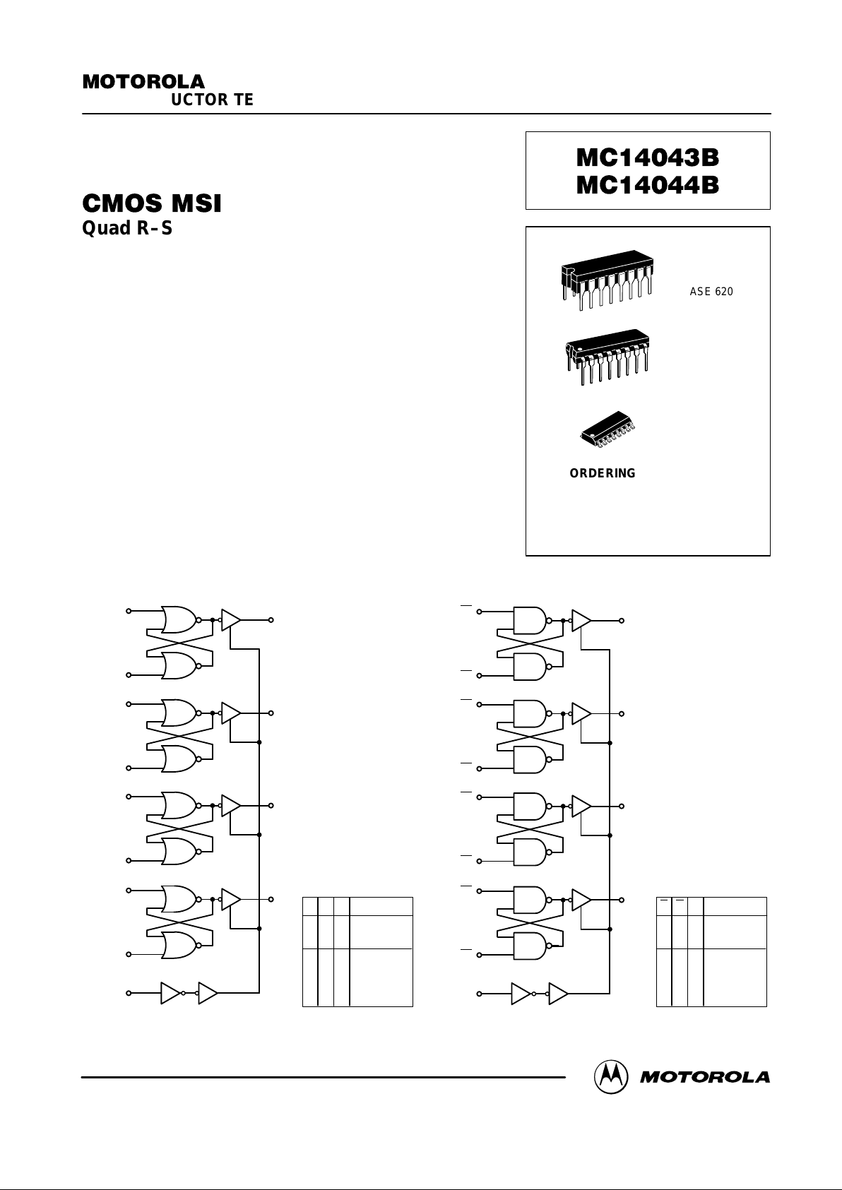
Quad R–S Latches
The MC14043B and MC14044B quad R–S latches are constructed with
MOS P–channel and N–channel enhancement mode devices in a single
monolithic structure. Each latch has an independent Q output and set and
reset inputs. The Q outputs are gated through three–state buffers having a
common enable input. The outputs are enabled with a logical “1” or high on
the enable input; a logical “0” or low d isconnects the latch from the Q
outputs, resulting in an open circuit at the Q outputs.
• Double Diode Input Protection
• Three–State Outputs with Common Enable
• Outputs Capable of Driving Two Low–power TTL Loads or One Low–
Power Schottky TTL Load Over the Rated Temperature Range
• Supply Voltage Range = 3.0 Vdc to 18 Vdc
MC14043B
TRUTH TABLE
X = Don’t Care
MC14044B
S R E Q
High
Impedance
X X 0
No Change
0
1
1
0
0
1
1
0
1
0
1
1
1
1
1
TRUTH TABLE
X = Don’t Care
S R E Q
High
Impedance
X X 0
0
1
0
No Change
0
0
1
1
0
1
0
1
1
1
1
1
ENABLE
R3
S3
R2
S2
R1
S1
R0
S0
4
3
6
7
12
11
14
15
5
Q3
Q2
Q1
Q0
2
9
10
1
ENABLE
S3
R3
S2
R2
S1
R1
S0
R0
4
3
6
7
12
11
14
15
5
Q3
Q2
Q1
Q0
13
9
10
1
VDD = PIN 16
VSS = PIN 8
NC = PIN 2
VDD = PIN 16
VSS = PIN 8
NC = PIN 13
SEMICONDUCTOR TECHNICAL DATA
Motorola, Inc. 1995
REV 3
1/94
L SUFFIX
CERAMIC
CASE 620
ORDERING INFORMATION
MC14XXXBCP Plastic
MC14XXXBCL Ceramic
MC14XXXBD SOIC
TA = – 55° to 125°C for all packages.
P SUFFIX
PLASTIC
CASE 648
D SUFFIX
SOIC
CASE 751B

MOTOROLA CMOS LOGIC DATA
163
MC14043B MC14044B
ELECTRICAL CHARACTERISTICS (Voltages Referenced to V
SS
)
V
– 55_C
25_C
125_C
Characteristic
Symbol
V
DD
Vdc
Min
Max
Min
Typ #
Max
Min
ÎÎÎ
ÎÎÎ
ÎÎÎ
Max
Unit
Output Voltage
“0” Level
Vin = VDD or 0
V
OL
5.0
10
15
—
—
—
0.05
0.05
0.05
—
—
—
0
0
0
0.05
0.05
0.05
—
—
—
ÎÎÎ
ÎÎÎ
ÎÎÎ
ÎÎÎ
0.05
0.05
0.05
Vdc
“1” Level
Vin = 0 or V
DD
V
OH
5.0
10
15
4.95
9.95
14.95
—
—
—
4.95
9.95
14.95
5.0
10
15
—
—
—
4.95
9.95
14.95
ÎÎÎ
ÎÎÎ
ÎÎÎ
ÎÎÎ
ÎÎÎ
—
—
—
Vdc
Input Voltage
“0” Level
(VO = 4.5 or 0.5 Vdc)
(VO = 9.0 or 1.0 Vdc)
(VO = 13.5 or 1.5 Vdc)
V
IL
5.0
10
15
—
—
—
1.5
3.0
4.0
—
—
—
2.25
4.50
6.75
1.5
3.0
4.0
—
—
—
ÎÎÎ
ÎÎÎ
ÎÎÎ
ÎÎÎ
ÎÎÎ
1.5
3.0
4.0
Vdc
“1” Level
(VO = 0.5 or 4.5 Vdc)
(VO = 1.0 or 9.0 Vdc)
(VO = 1.5 or 13.5 Vdc)
V
IH
5.0
10
15
3.5
7.0
11
—
—
—
3.5
7.0
11
2.75
5.50
8.25
—
—
—
3.5
7.0
11
ÎÎÎ
ÎÎÎ
ÎÎÎ
ÎÎÎ
ÎÎÎ
—
—
—
Vdc
Output Drive Current
(VOH = 2.5 Vdc) Source
(VOH = 4.6 Vdc)
(VOH = 9.5 Vdc)
(VOH = 13.5 Vdc)
I
OH
5.0
5.0
10
15
– 3.0
– 0.64
– 1.6
– 4.2
—
—
—
—
– 2.4
– 0.51
– 1.3
– 3.4
– 4.2
– 0.88
– 2.25
– 8.8
—
—
—
—
– 1.7
– 0.36
– 0.9
– 2.4
ÎÎÎ
ÎÎÎ
ÎÎÎ
ÎÎÎ
ÎÎÎ
—
—
—
—
mAdc
(VOL = 0.4 Vdc) Sink
(VOL = 0.5 Vdc)
(VOL = 1.5 Vdc)
I
OL
5.0
10
15
0.64
1.6
4.2
—
—
—
0.51
1.3
3.4
0.88
2.25
8.8
—
—
—
0.36
0.9
2.4
ÎÎÎ
ÎÎÎ
ÎÎÎ
ÎÎÎ
ÎÎÎ
—
—
—
mAdc
Input Current
I
in
15
—
± 0.1
—
±0.00001
± 0.1
—
ÎÎÎ
ÎÎÎ
ÎÎÎ
± 1.0
µAdc
Input Capacitance
(Vin = 0)
C
in
—
—
—
—
5.0
7.5
—
ÎÎÎ
ÎÎÎ
ÎÎÎ
—
pF
Quiescent Current
(Per Package)
I
DD
5.0
10
15
—
—
—
1.0
2.0
4.0
—
—
—
0.002
0.004
0.006
1.0
2.0
4.0
—
—
—
ÎÎÎ
ÎÎÎ
ÎÎÎ
ÎÎÎ
ÎÎÎ
30
60
120
µAdc
Total Supply Current**†
(Dynamic plus Quiescent,
Per Package)
(CL = 50 pF on all outputs all
buffers switching)
I
T
5.0
10
15
IT = (0.58 µA/kHz) f + I
DD
IT = (1.15 µA/kHz) f + I
DD
IT = (1.73 µA/kHz) f + I
DD
µAdc
Three–State Output Leakage
Current
I
TL
15
—
± 0.1
—
± 0.0001
± 0.1
—
ÎÎÎ
ÎÎÎ
ÎÎÎ
ÎÎÎ
± 3.0
µAdc
#Data labelled “Typ” is not to be used for design purposes but is intended as an indication of the IC’s potential performance.
**The formulas given are for the typical characteristics only at 25_C.
†To calculate total supply current at loads other than 50 pF:
IT(CL) = IT(50 pF) + (CL – 50) Vfk
where: IT is in µA (per package), CL in pF, V = (VDD – VSS) in volts, f in kHz is input frequency, and k = 0.004.
*Maximum Ratings are those values beyond which damage to the device may occur.
†Temperature Derating: Plastic “P and D/DW” Packages: – 7.0 mW/_C From 65_C To 125_C
Ceramic “L” Packages – 12 mW/_C From 100_C To 125_C
 Loading...