

Motorola MC1403P1, MC1403D, MC1403BD Datasheet
Order this document by MC1403/D
A precision band–gap voltage reference designed for critical
instrumentation and D/A converter applications. This unit is designed to work
with D/A converters, up to 12 bits in accuracy, or as a reference for power
supply applications.
• Output Voltage: 2.5 V
• Input Voltage Range: 4.5 V to 40 V
• Quiescent Current: 1.2 mA Typical
• Output Current: 10 mA
• Temperature Coefficient: 10 ppm/°C Typical
• Guaranteed Temperature Drift Specification
• Equivalent to AD580
• Standard 8–Pin DIP, and 8–Pin SOIC Package
T ypical Applications
• Voltage Reference for 8 to 12 Bit D/A Converters
• Low T
Zener Replacement
C
• High Stability Current Reference
• Voltmeter System Reference
MAXIMUM RATINGS
Input Voltage V
Storage Temperature T
Junction Temperature T
Operating Ambient Temperature Range
MC1403B
MC1403
"
25 mV
(TA = 25°C, unless otherwise noted.)
Rating
Symbol Value Unit
40 V
–65 to 150 °C
+175 °C
–40 to +85
0 to +70
°C
°C
T
I
stg
J
A
PRECISION LOW VOLTAGE
REFERENCE
SEMICONDUCTOR
TECHNICAL DATA
P1 SUFFIX
PLASTIC PACKAGE
8
1
8
ORDERING INFORMATION
Device
MC1403D
MC1403P1
MC1403BD
MC1403BP1
1
PIN CONNECTIONS
1
V
in
2
V
out
3
Gnd
4
NC
Temperature Range
TA = 0° to +70°C
TA = –40° to +85°C
CASE 626
D SUFFIX
PLASTIC PACKAGE
CASE 751
(SO–8)
7
6
5
Operating
NC8
NC
NC
NC
Package
SO–8
Plastic DIP
SO–8
Plastic DIP
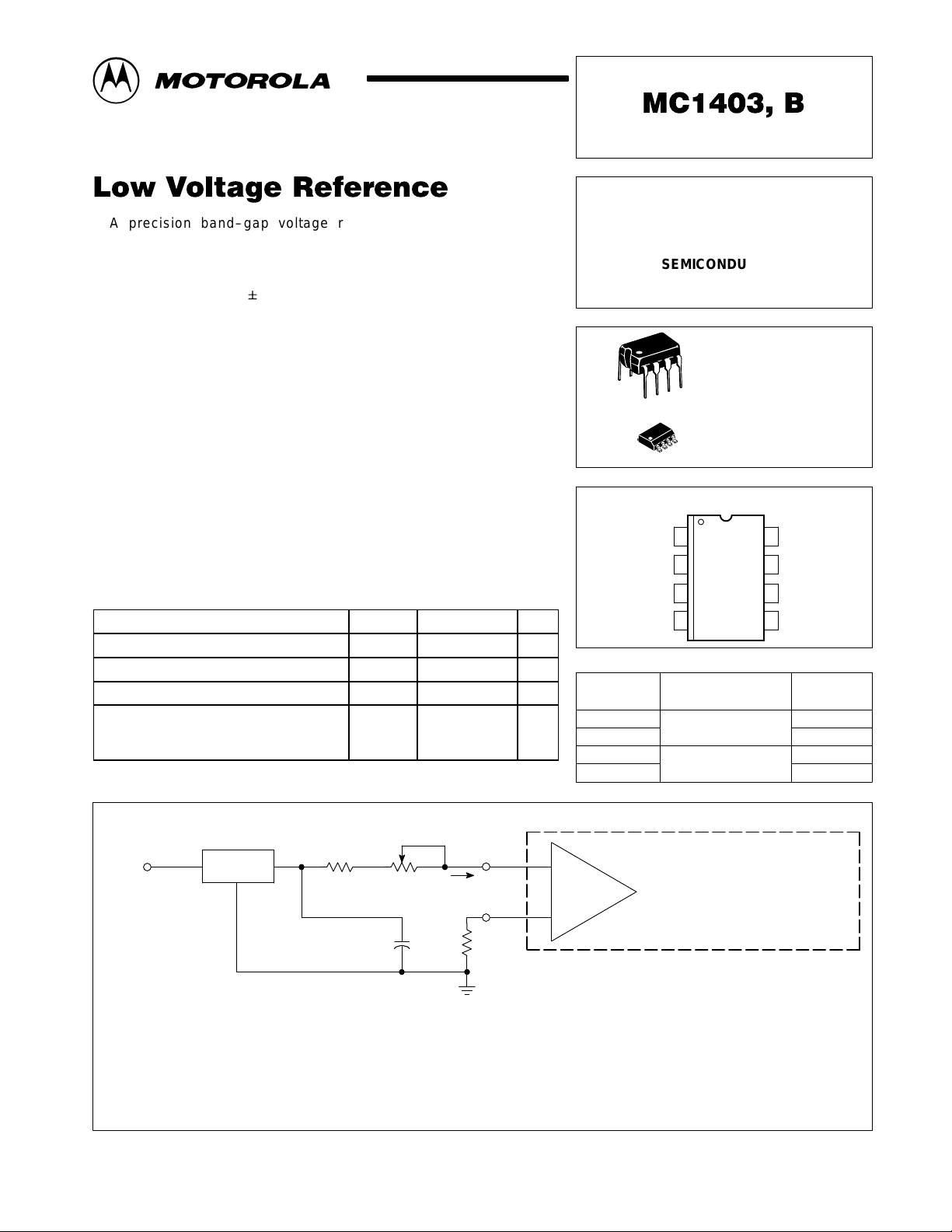
Figure 1. A Reference for Monolithic D/A Converters
2.5 V
1
+5.0 V
Providing the Reference Current
for Motorola Monolithic D/A Converters
The MC1403 makes an ideal reference for many monolithic D/A converters, requiring a stable current reference of
nominally 2.0 mA. This can be easily obtained from the
MC1403 with the addition of a series resistor, R1. A variable
resistor, R2, is recommended to provide means for full–
scale adjust on the D/A converter.
MC1403
2
3
1.0 k
*0.1
C1
MOTOROLA ANALOG IC DEVICE DATA
Full Scale
Adjust 500
R2R1
µ
F
I
Ref
Ω
Reference
Amplifier
1.2 k
R3
* Caution: System stability may be affected if output capacitance
* exceeds 1.0 µF. Using higher capacitance values is not
* recommended and should be carefully considered.
The resistor R3 improves temperature performance by
matching the impedance on both inputs of the D/A reference
amplifier. The capacitor decouples any noise present on the
reference line. It is essential if the D/A converter is located
any appreciable distance from the reference.
A single MC1403 reference can provide the required
current input for up to five of the monolithic D/A converters.
Motorola, Inc. 1996 Rev 1
Monolithic D/A
Converter
1
MC1403, B
ELECTRICAL CHARACTERISTICS
Characteristic
Output Voltage V
(IO = 0 mA)
Temperature Coefficient of Output Voltage* ∆VO/∆T – 10 40 ppm/°C
MC1403
Output Voltage Change* ∆V
(Over specified temperature range)
MC1403B 0 to +70°C
MC1403B –40 to +85°C
Line Regulation (IO = 0 mA) Reg
(15 V VI 40 V)
(4.5 V VI 15 V)
Load Regulation Reg
(0 mA < IO < 10 mA)
Quiescent Current I
(IO = 0 mA)
*This test is not applicable to the MC1403D or MC1403BD surface mount devices.
(Vin = 15 V, TA = 25°C, unless otherwise noted.)
Symbol Min Typ Max Unit
out
O
line
load
Q
2.475 2.5 2.525 V
–
–
–
–
– – 10 mV
– 1.2 1.5 mA
1.2
0.6
mV
–
–
7.0
12.5
mV
4.5
3.0
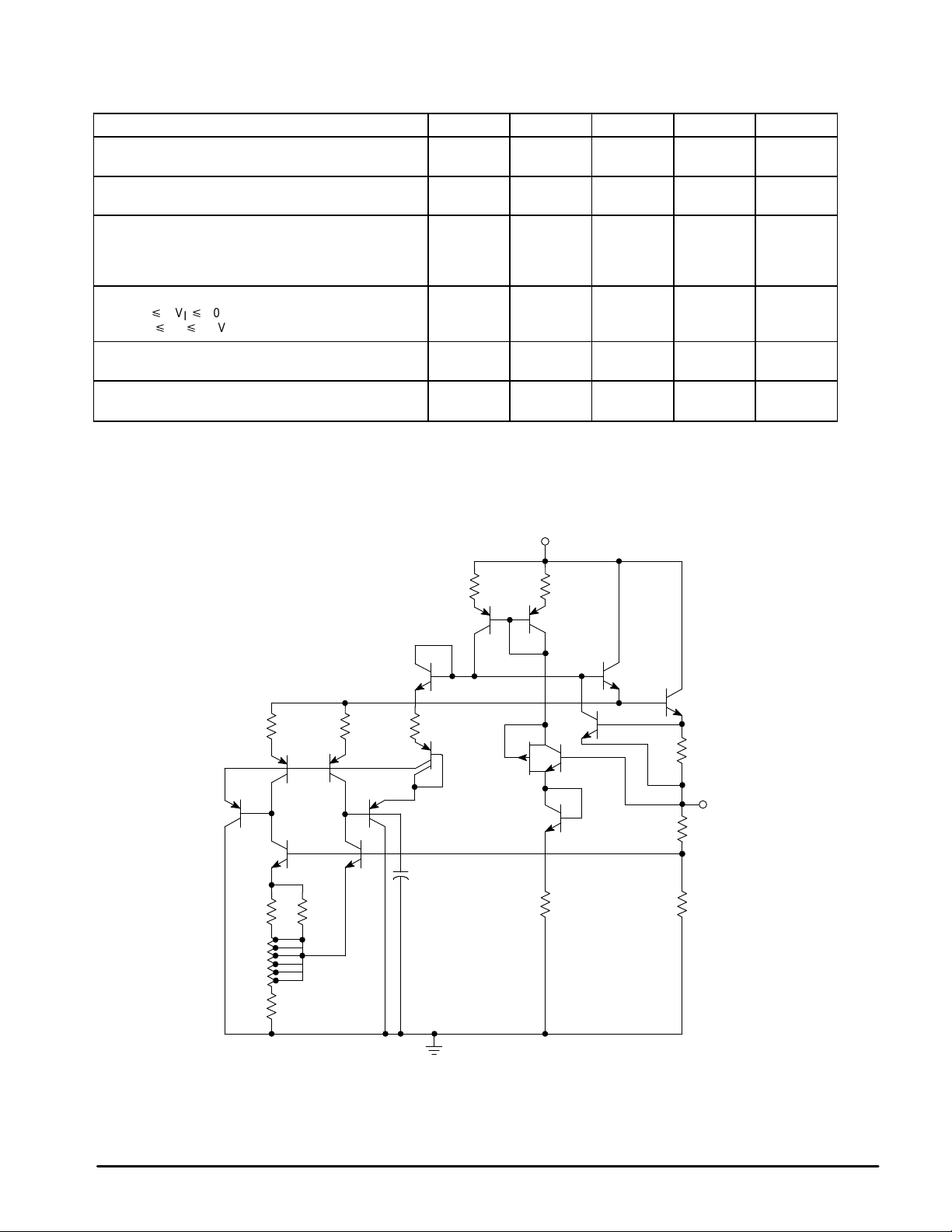
Figure 2. MC1403, B Schematic
V
in
2.37 k
1.0 k
5.61 k
2.0 k
1.73 k
1.0 k2.0 k
C1
30 pF
2.0 k2.0 k
32
V
out
1.5 k
1.483 k10 k
This device contains 15 active transistors.
2
MOTOROLA ANALOG IC DEVICE DATA
MC1403, B
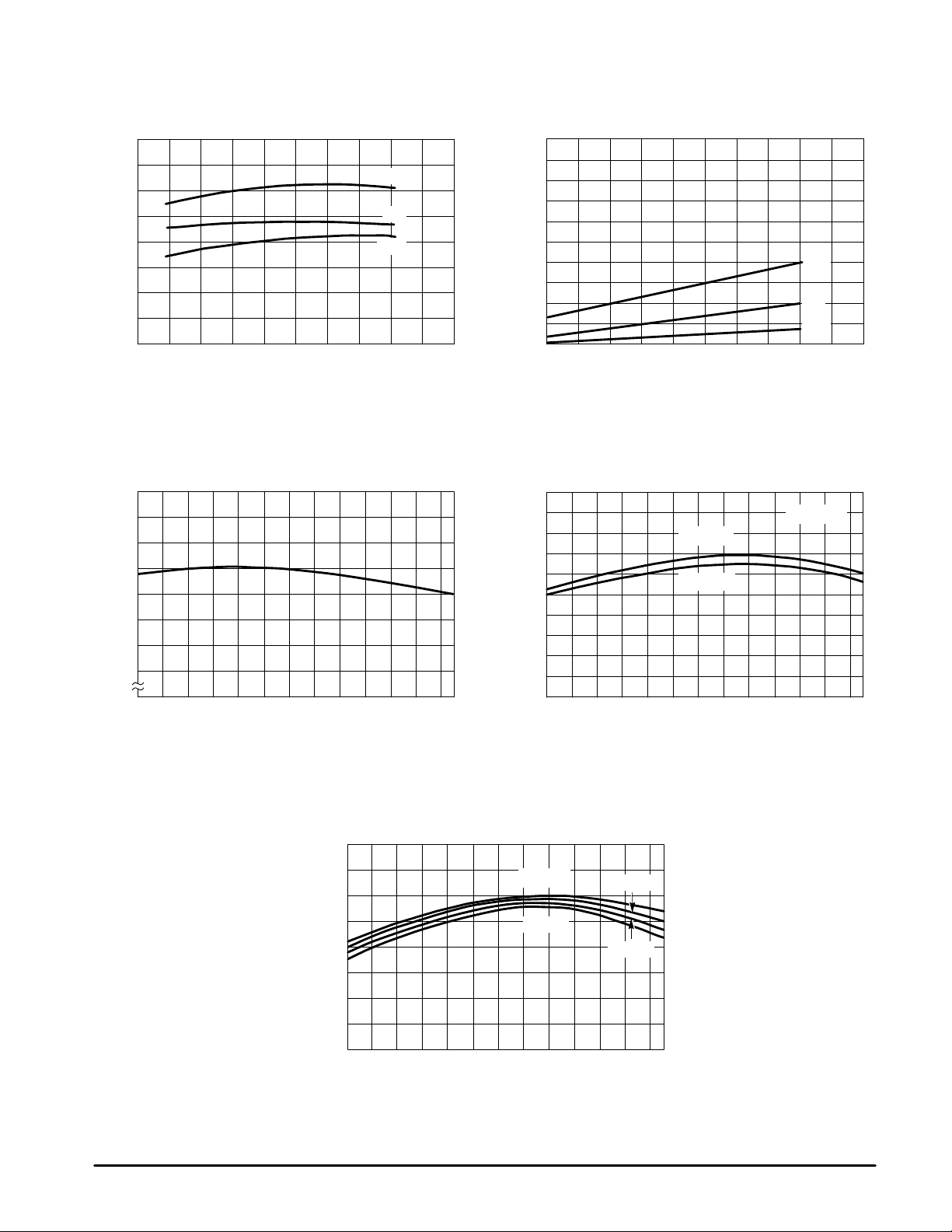
Figure 3. T ypical Change in V
(Normalized to Vin = 15 V @ TC = 25°C)
2.0
1.0
(mV)
0
out
–1.0
–2.0
–3.0
–4.0
out
V , CHANGE IN V
∆
–5.0
–6.0
01020304050
Vin, INPUT VOLTAGE (V)
versus V
out
in
25°C
0°C
75°C
Figure 4. Change in Output Voltage
versus Load Current
(Normalized to V
10
9.0
8.0
7.0
6.0
5.0
4.0
3.0
2.0
, CHANGE IN OUTPUT VOLTAGE (mV)
1.0
out
V
∆
0
0 1.0 2.0 3.0 4.0 5.0 6.0 7.0 8.0 9.0 10
I
out
@ Vin = 15 V, I
out
, OUTPUT CURRENT (mA)
= 0 mA)
out
75°C
0°C
25°C
Figure 5. Quiescent Current versus T emperature
1.25
1.20
1.15
1.10
1.05
1.00
0.95
, QUIESCENT CURRENT (mA)
1
I
0.90
(Vin = 15 V, I
0
TA, TEMPERATURE (°C)
= 0 mA)
out
Figure 7. Change in V
(Normalized to TA = 25°C, Vin = 15 V, I
4.0
2.0
(mV)
0
out
–2.0
–4.0
–6.0
–8.0
out
V , CHANGE IN V
∆
–10
–12
(mV)
out
out
V , CHANGE IN V
∆
806040200–40 –20
8570503010–10–30
out
TA, TEMPERATURE (
Figure 6. Change in V
(Normalized to V
0
–2.0
–4.0
–6.0
–8.0
–10
–12
–14
versus T emperature
= 0 mA)
out
IO = 0 mA
= 8.0 mA
°
C)
= 2.0 mA
= 5.0 mA
70503010–10–30
versus T emperature
out
@ Vin = 15 V)
out
Vin = 15 V
Vin = 5.0 V
TA, TEMPERATURE (
85
806040200–40 –20
I
= 2 mA
out
806040200–40 –20 8570503010–10–30
°
C)
MOTOROLA ANALOG IC DEVICE DATA
3
 Loading...