

Order this document by MC1403/D
A precision band–gap voltage reference designed for critical
instrumentation and D/A converter applications. This unit is designed to work
with D/A converters, up to 12 bits in accuracy, or as a reference for power
supply applications.
• Output Voltage: 2.5 V
• Input Voltage Range: 4.5 V to 40 V
• Quiescent Current: 1.2 mA Typical
• Output Current: 10 mA
• Temperature Coefficient: 10 ppm/°C Typical
• Guaranteed Temperature Drift Specification
• Equivalent to AD580
• Standard 8–Pin DIP, and 8–Pin SOIC Package
T ypical Applications
• Voltage Reference for 8 to 12 Bit D/A Converters
• Low T
Zener Replacement
C
• High Stability Current Reference
• Voltmeter System Reference
MAXIMUM RATINGS
Input Voltage V
Storage Temperature T
Junction Temperature T
Operating Ambient Temperature Range
MC1403B
MC1403
"
25 mV
(TA = 25°C, unless otherwise noted.)
Rating
Symbol Value Unit
40 V
–65 to 150 °C
+175 °C
–40 to +85
0 to +70
°C
°C
T
I
stg
J
A
PRECISION LOW VOLTAGE
REFERENCE
SEMICONDUCTOR
TECHNICAL DATA
P1 SUFFIX
PLASTIC PACKAGE
8
1
8
ORDERING INFORMATION
Device
MC1403D
MC1403P1
MC1403BD
MC1403BP1
1
PIN CONNECTIONS
1
V
in
2
V
out
3
Gnd
4
NC
Temperature Range
TA = 0° to +70°C
TA = –40° to +85°C
CASE 626
D SUFFIX
PLASTIC PACKAGE
CASE 751
(SO–8)
7
6
5
Operating
NC8
NC
NC
NC
Package
SO–8
Plastic DIP
SO–8
Plastic DIP
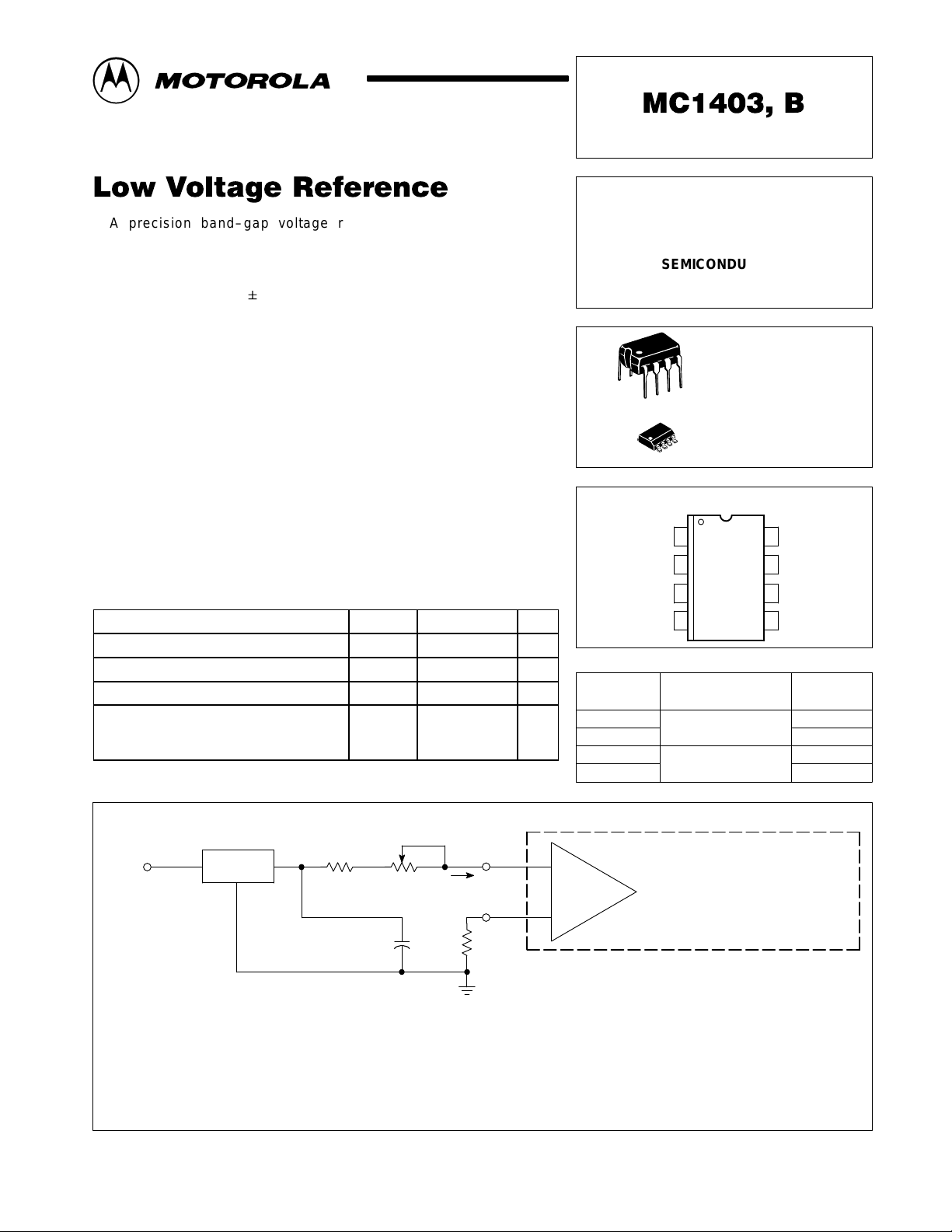
Figure 1. A Reference for Monolithic D/A Converters
2.5 V
1
+5.0 V
Providing the Reference Current
for Motorola Monolithic D/A Converters
The MC1403 makes an ideal reference for many monolithic D/A converters, requiring a stable current reference of
nominally 2.0 mA. This can be easily obtained from the
MC1403 with the addition of a series resistor, R1. A variable
resistor, R2, is recommended to provide means for full–
scale adjust on the D/A converter.
MC1403
2
3
1.0 k
*0.1
C1
MOTOROLA ANALOG IC DEVICE DATA
Full Scale
Adjust 500
R2R1
µ
F
I
Ref
Ω
Reference
Amplifier
1.2 k
R3
* Caution: System stability may be affected if output capacitance
* exceeds 1.0 µF. Using higher capacitance values is not
* recommended and should be carefully considered.
The resistor R3 improves temperature performance by
matching the impedance on both inputs of the D/A reference
amplifier. The capacitor decouples any noise present on the
reference line. It is essential if the D/A converter is located
any appreciable distance from the reference.
A single MC1403 reference can provide the required
current input for up to five of the monolithic D/A converters.
Motorola, Inc. 1996 Rev 1
Monolithic D/A
Converter
1
MC1403, B
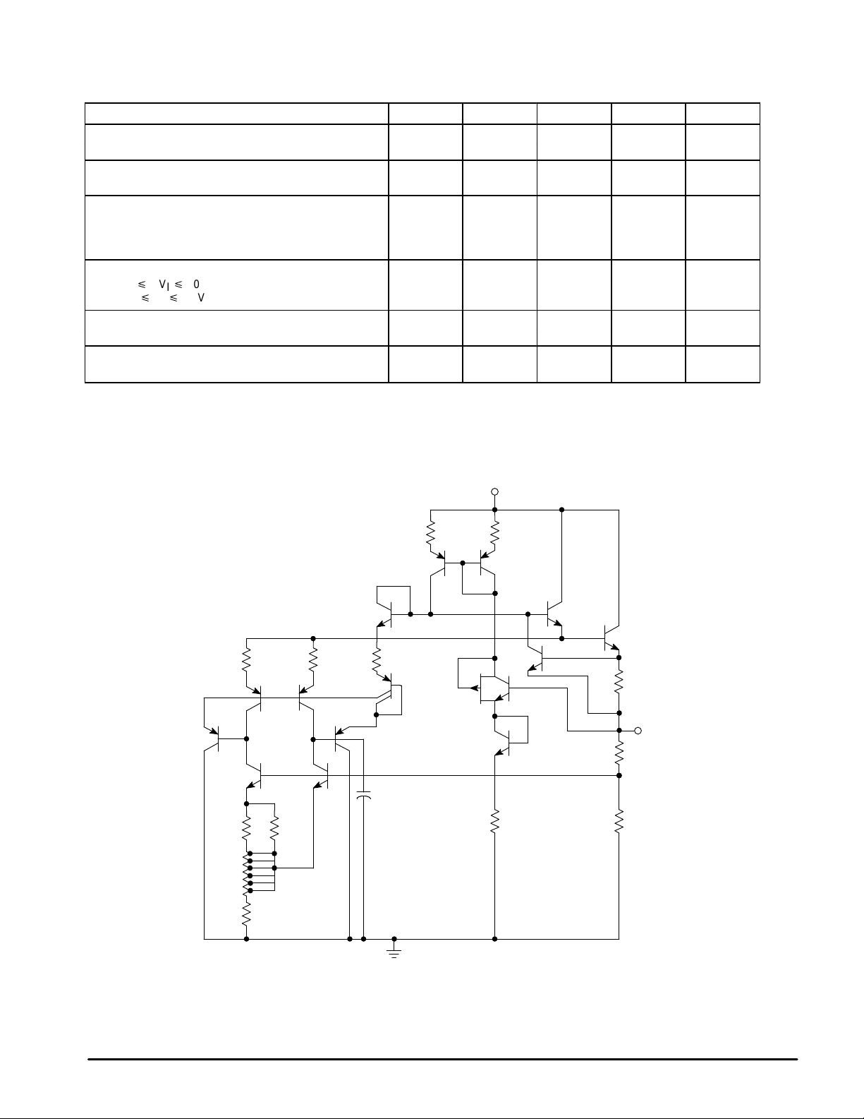
ELECTRICAL CHARACTERISTICS
Characteristic
Output Voltage V
(IO = 0 mA)
Temperature Coefficient of Output Voltage* ∆VO/∆T – 10 40 ppm/°C
MC1403
Output Voltage Change* ∆V
(Over specified temperature range)
MC1403B 0 to +70°C
MC1403B –40 to +85°C
Line Regulation (IO = 0 mA) Reg
(15 V VI 40 V)
(4.5 V VI 15 V)
Load Regulation Reg
(0 mA < IO < 10 mA)
Quiescent Current I
(IO = 0 mA)
*Guaranteed but not tested.
(Vin = 15 V, TA = 25°C, unless otherwise noted.)
Symbol Min Typ Max Unit
out
O
line
load
Q
2.475 2.5 2.525 V
–
–
–
–
– – 10 mV
– 1.2 1.5 mA
1.2
0.6
mV
–
–
7.0
12.5
mV
4.5
3.0
Figure 2. MC1403, B Schematic
V
in
2.37 k
1.0 k
5.61 k
2.0 k
1.73 k
1.0 k2.0 k
C1
30 pF
2.0 k2.0 k
32
V
out
1.5 k
1.483 k10 k
This device contains 15 active transistors.
2
MOTOROLA ANALOG IC DEVICE DATA
MC1403, B
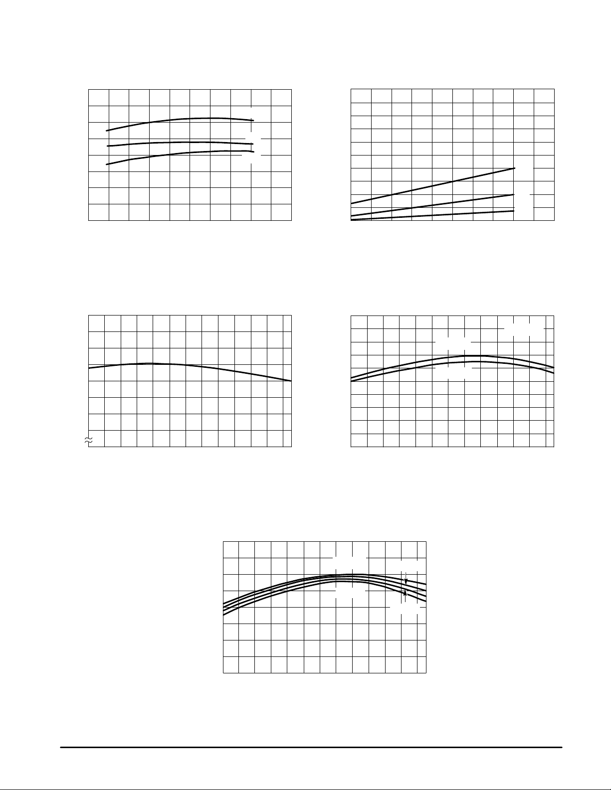
Figure 3. T ypical Change in V
(Normalized to Vin = 15 V @ TC = 25°C)
2.0
1.0
(mV)
0
out
–1.0
–2.0
–3.0
–4.0
out
V , CHANGE IN V
∆
–5.0
–6.0
01020304050
Vin, INPUT VOLTAGE (V)
versus V
out
in
25°C
0°C
75°C
Figure 4. Change in Output Voltage
versus Load Current
(Normalized to V
10
9.0
8.0
7.0
6.0
5.0
4.0
3.0
2.0
, CHANGE IN OUTPUT VOLTAGE (mV)
1.0
out
V
∆
0
0 1.0 2.0 3.0 4.0 5.0 6.0 7.0 8.0 9.0 10
I
out
@ Vin = 15 V, I
out
, OUTPUT CURRENT (mA)
= 0 mA)
out
75°C
0°C
25°C
Figure 5. Quiescent Current versus T emperature
1.25
1.20
1.15
1.10
1.05
1.00
0.95
, QUIESCENT CURRENT (mA)
1
I
0.90
(Vin = 15 V, I
0
TA, TEMPERATURE (°C)
= 0 mA)
out
Figure 7. Change in V
(Normalized to TA = 25°C, Vin = 15 V, I
4.0
2.0
(mV)
0
out
–2.0
–4.0
–6.0
–8.0
out
V , CHANGE IN V
∆
–10
–12
(mV)
out
out
V , CHANGE IN V
∆
806040200–40 –20
8570503010–10–30
out
TA, TEMPERATURE (
Figure 6. Change in V
(Normalized to V
0
–2.0
–4.0
–6.0
–8.0
–10
–12
–14
versus T emperature
= 0 mA)
out
IO = 0 mA
= 8.0 mA
°
C)
= 2.0 mA
= 5.0 mA
70503010–10–30
versus T emperature
out
@ Vin = 15 V)
out
Vin = 15 V
Vin = 5.0 V
TA, TEMPERATURE (
85
806040200–40 –20
I
= 2 mA
out
806040200–40 –20 8570503010–10–30
°
C)
MOTOROLA ANALOG IC DEVICE DATA
3

MC1403, B
3–1/2–Digit Voltmeter – Common Anode
Displays, Flashing Overrange
An example of a 3–1/2–digit voltmeter using the MC14433
is shown in the circuit diagram of Figure 8. The reference
voltage for the system uses an MC1403 2.5 V reference IC.
The full scale potentiometer can calibrate for a full scale of
199.9 mV or 1.999 V. When switching from 2.0 V to 200 mV
operation, RI is also changed, as shown on the diagram.
When using RC equal to 300 kΩ, the clock frequency for
the system is about 66 kHz. The resulting conversion time is
approximately 250 ms.
When the input is overrange, the display flashes on and
off. The flashing rate is one–half the conversion rate. This is
Figure 8. 3–1/2–Digit V oltmeter
+5.0 V
0.1µF
V
X
* RI = 470 k
RI = 27 k
** Mylar Capacitor
MC1403
1
0.1 µF **
0.1
Ω
Ω
for 200 mV Range
2
3
RI *
for 2.0 V Range
0.1
300 k
µ
F
R
3
1
4
5
6
7
8
µ
F
C
20 k
21011
MC14433
19
DS1
DS2
12
DS3
24
16171815
DS4
23
22
21
20
13
9
14
0.1
µ
F
+5.0 V
–5.0 V
–5.0 V
–5.0 V
0.1
–5.0 V –5.0 V
5
D
3
CQ
4
9
D
11
C
710
done by dividing the EOC pulse rate by 2 with 1/2 MC14013B
flip–flop and blanking the display using the blanking input of
the MC14543B.
The display uses an LED display with common anode digit
lines driven with an MC14543B decoder and an MC1413
LED driver. The MC1413 contains 7 Darlington transistor
drivers and resistors to drive the segments of the display . The
digit drive is provided by four MPS–A12 Darlington
transistors operating in an emitter–follower configuration.
The MC14543B, MC14013B and LED displays are
referenced to VEE via Pin 13 of the MC14433. This places the
full power supply voltage across the display. The current for
the display may be adjusted by the value of the segment
resistors shown as 150 Ω in Figure 8.
+5.0 V +5.0 V
µ
F
6
S
R
S
R
4
2
3
5
8
5.0 V
Q
13
Q
12
Q
14
161
9
10
11
12
13
MC14543B
14
15
6
7
1
2
MC14013B
8
+5.0 V
7
6
5
4
3
2
1
–5.0 V
–5.0 V
50 µF
–5.0 V
MC1413
MPS–A12
51 k
+5.0 V
Segment Resistors
150
10
11
12
13
14
15
16
Minus Sign
200
Plus Sign
110
Common
Anode
LED
Display
µ
F
0.1
Ω
(7)
Ω
Ω
bacdegf
MPS–A12
(4)
4
MOTOROLA ANALOG IC DEVICE DATA
NOTE 2
–T–
SEATING
PLANE
H
58
–B–
14
F
–A–
C
N
D
K
G
0.13 (0.005) B
M
T
MC1403, B
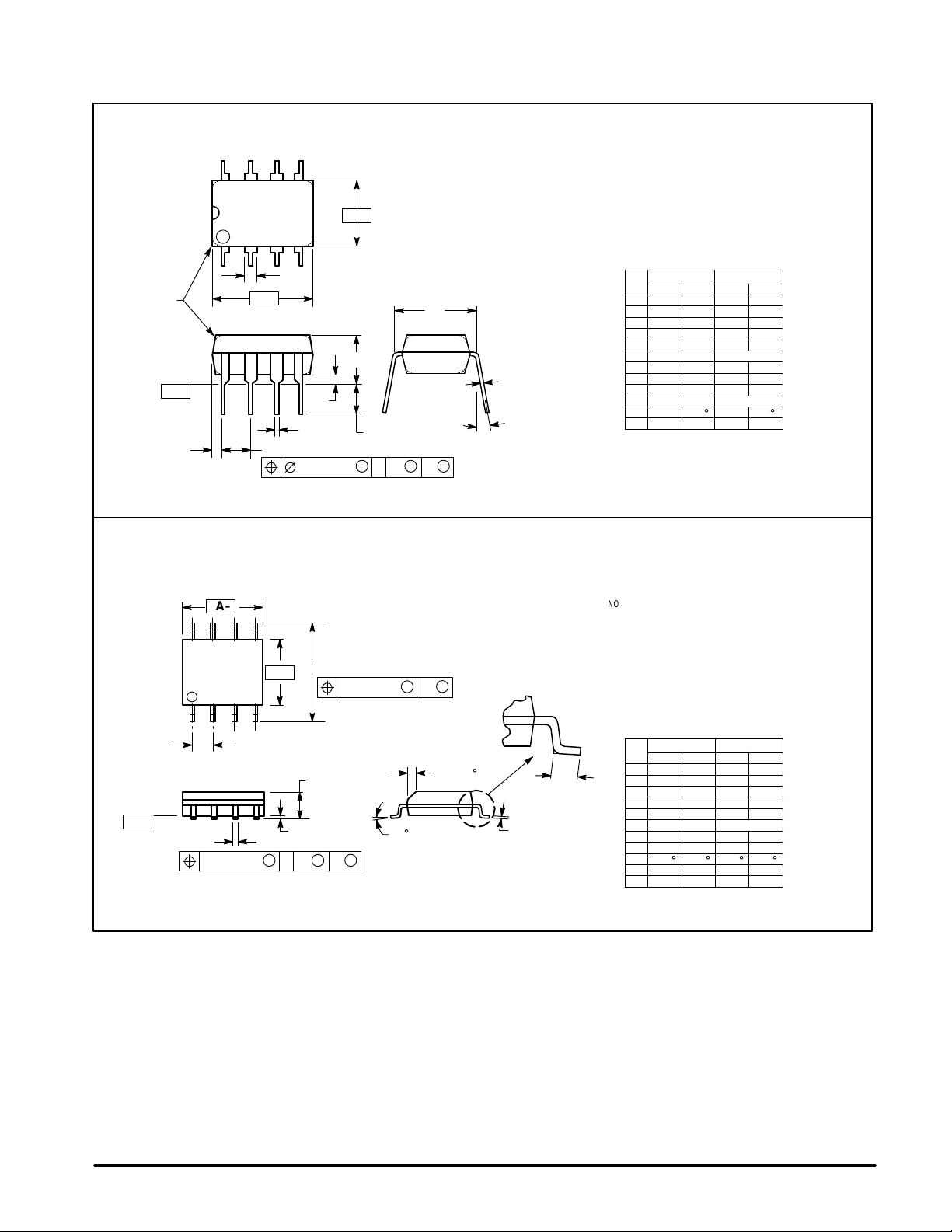
OUTLINE DIMENSIONS
P1 SUFFIX
PLASTIC PACKAGE
CASE 626–05
ISSUE K
L
J
M
M
A
M
NOTES:
1. DIMENSION L TO CENTER OF LEAD WHEN
FORMED PARALLEL.
2. PACKAGE CONTOUR OPTIONAL (ROUND OR
SQUARE CORNERS).
3. DIMENSIONING AND TOLERANCING PER ANSI
Y14.5M, 1982.
DIM MIN MAX MIN MAX
A 9.40 10.16 0.370 0.400
B 6.10 6.60 0.240 0.260
C 3.94 4.45 0.155 0.175
D 0.38 0.51 0.015 0.020
F 1.02 1.78 0.040 0.070
G 2.54 BSC 0.100 BSC
H 0.76 1.27 0.030 0.050
J 0.20 0.30 0.008 0.012
K 2.92 3.43 0.115 0.135
L 7.62 BSC 0.300 BSC
M ––– 10 ––– 10
N 0.76 1.01 0.030 0.040
INCHESMILLIMETERS
__
–T–
–A–
58
4X P
–B–
14
G
C
SEATING
PLANE
8X D
K
0.25 (0.010)MB
SS
A0.25 (0.010)MTB
D SUFFIX
PLASTIC PACKAGE
CASE 751–05
ISSUE N
M
R
X 45
_
M
(SO–8)
_
NOTES:
1. DIMENSIONING AND TOLERANCING PER
ANSI Y14.5M, 1982.
2. CONTROLLING DIMENSION: MILLIMETER.
3. DIMENSIONS A AND B DO NOT INCLUDE
MOLD PROTRUSION.
4. MAXIMUM MOLD PROTRUSION 0.15 (0.006)
PER SIDE.
5. DIMENSION D DOES NOT INCLUDE DAMBAR
PROTRUSION. ALLOWABLE DAMBAR
PROTRUSION SHALL BE 0.127 (0.005) TOTAL
IN EXCESS OF THE D DIMENSION AT
MAXIMUM MATERIAL CONDITION.
DIM MIN MAX MIN MAX
F
J
A 4.80 5.00 0.189 0.196
B 3.80 4.00 0.150 0.157
C 1.35 1.75 0.054 0.068
D 0.35 0.49 0.014 0.019
F 0.40 1.25 0.016 0.049
G 1.27 BSC 0.050 BSC
J 0.18 0.25 0.007 0.009
K 0.10 0.25 0.004 0.009
M 0 7 0 7
P 5.80 6.20 0.229 0.244
R 0.25 0.50 0.010 0.019
INCHESMILLIMETERS
____
MOTOROLA ANALOG IC DEVICE DATA
5

MC1403, B
NOTES
6
MOTOROLA ANALOG IC DEVICE DATA

MC1403, B
NOTES
MOTOROLA ANALOG IC DEVICE DATA
7

MC1403, B
Motorola reserves the right to make changes without further notice to any products herein. Motorola makes no warranty , representation or guarantee regarding
the suitability of its products for any particular purpose, nor does Motorola assume any liability arising out of the application or use of any product or circuit, and
specifically disclaims any and all liability, including without limitation consequential or incidental damages. “T ypical” parameters which may be provided in Motorola
data sheets and/or specifications can and do vary in different applications and actual performance may vary over time. All operating parameters, including “Typicals”
must be validated for each customer application by customer’s technical experts. Motorola does not convey any license under its patent rights nor the rights of
others. Motorola products are not designed, intended, or authorized for use as components in systems intended for surgical implant into the body, or other
applications intended to support or sustain life, or for any other application in which the failure of the Motorola product could create a situation where personal injury
or death may occur. Should Buyer purchase or use Motorola products for any such unintended or unauthorized application, Buyer shall indemnify and hold Motorola
and its officers, employees, subsidiaries, affiliates, and distributors harmless against all claims, costs, damages, and expenses, and reasonable attorney fees
arising out of, directly or indirectly, any claim of personal injury or death associated with such unintended or unauthorized use, even if such claim alleges that
Motorola was negligent regarding the design or manufacture of the part. Motorola and are registered trademarks of Motorola, Inc. Motorola, Inc. is an Equal
Opportunity/Affirmative Action Employer.
How to reach us:
USA/EUROPE/Locations Not Listed: Motorola Literature Distribution; JAPAN: Motorola Japan Ltd.; SPD, Strategic Planning Office, 141,
P.O. Box 5405, Denver, Colorado 80217. 1–303–675–2140 or 1–800–441–2447 4–32–1 Nishi–Gotanda, Shinagawa–ku, Tokyo, Japan. 81–3–5487–8488
Customer Focus Center: 1–800–521–6274
Mfax: RMFAX0@email.sps.mot.com – TOUCHTONE 1–602–244–6609 ASIA/P ACIFIC: Motorola Semiconductors H.K. Ltd.; Silicon Harbour Centre,
Motorola Fax Back System – US & Canada ONLY 1–800–774–1848 2, Dai King Street, Tai Po Industrial Estate, Tai Po, N.T., Hong Kong.
HOME PAGE: http://motorola.com/sps/
8
– http://sps.motorola.com/mfax/ 852–26629298
◊
MOTOROLA ANALOG IC DEVICE DATA
Mfax is a trademark of Motorola, Inc.
MC1403/D
 Loading...