

Motorola MC14034BCL, MC14034BCP, MC14034BDW Datasheet
MOTOROLA CMOS LOGIC DATA
135
MC14034B
The MC14034B is a bidirectional 8–bit static parallel/serial, input/output
bus register. The device contains two sets of input/output lines which allows
the bidirectional transfer of data between two buses; the conversion of serial
data t o parallel form, or t he conversion of parallel data to serial form.
Additionally the serial data input allows data to be entered shift/right, while
shift/left can be accomplished by hard–wiring each parallel output to the
previous parallel bit input.
Other useful applications for this device include pseudo–random code
generation, sample and hold register, frequency and phase–comparator,
address or buffer register, and serial/parallel input/output conversions.
• Bidirectional Parallel Data Input
• Diode Protection on All Inputs
• Supply Voltage Range = 3.0 Vdc to 18 Vdc
• Capable of Driving Two Low–power TTL Loads or One Low–power
Schottky TTL Load Over the Rated Temperature Range.
• Pin–for–Pin Replacement for CD4034B.
MAXIMUM RATINGS* (Voltages Referenced to V
SS
)
Symbol
Parameter
Value
Unit
V
DD
DC Supply Voltage
– 0.5 to + 18.0
V
Vin, V
out
Input or Output Voltage (DC or Transient)
– 0.5 to VDD + 0.5
V
lin, l
out
Input or Output Current (DC or Transient),
per Pin
± 10
mA
P
D
Power Dissipation, per Package†
500
mW
T
stg
Storage Temperature
– 65 to + 150
_
C
T
L
Lead Temperature (8–Second Soldering)
260
_
C
*Maximum Ratings are those values beyond which damage to the device may occur.
†Temperature Derating:
Plastic “P and D/DW” Packages: – 7.0 mW/_C From 65_C To 125_C
Ceramic “L” Packages: – 12 mW/_C From 100_C To 125_C
This device contains protection circuitry to guard against damage
due to high static voltages or electric fields. However, precautions must
be taken to avoid applications of any voltage higher than maximum rated
voltages to this high-impedance circuit. For proper operation, Vin and
V
out
should be constrained to the range VSS ≤ (Vin or V
out
) ≤ VDD.
Unused inputs must always be tied to an appropriate logic voltage
level (e.g., either VSS or VDD). Unused outputs must be left open.
SEMICONDUCTOR TECHNICAL DATA
Motorola, Inc. 1995
REV 3
1/94
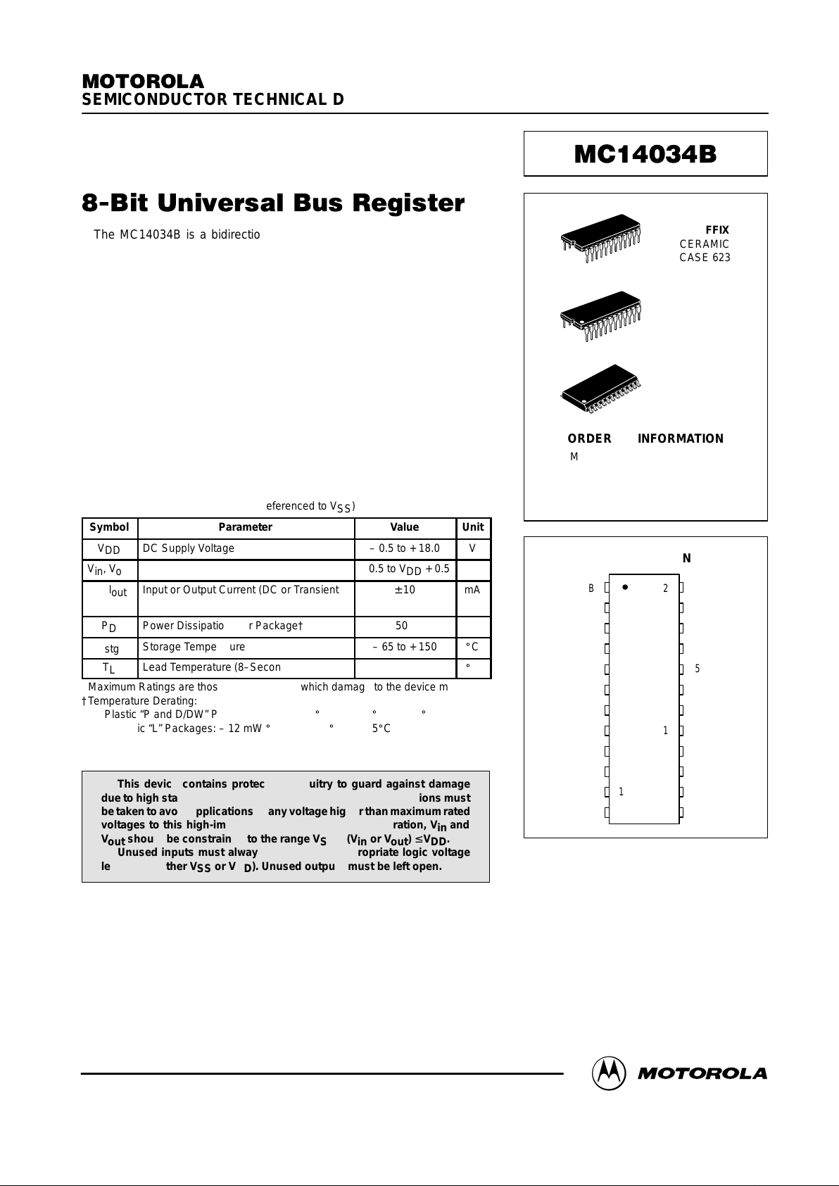
L SUFFIX
CERAMIC
CASE 623
ORDERING INFORMATION
MC14XXXBCP Plastic
MC14XXXBCL Ceramic
MC14XXXBDW SOIC
TA = – 55° to 125°C for all packages.
P SUFFIX
PLASTIC
CASE 709
DW SUFFIX
SOIC
CASE 751E
PIN ASSIGNMENT
B3
B5
B6
B7
B8
B1
B2
B4 A5
A6
A7
A8
V
DD
C
A1
A2
5
4
3
2
1
10
9
8
7
6
14
15
16
17
18
19
20
13
11
12
21
22
23
24
P/S
A/S
A3
A4
A/B
V
SS
D
S
A ENABLE
MOTOROLA CMOS LOGIC DATAMC14034B
136
ELECTRICAL CHARACTERISTICS (Voltages Referenced to V
SS
)
V
– 55_C
25_C
125_C
Characteristic
Symbol
V
DD
Vdc
Min
Max
Min
Typ #
Max
Min
ÎÎÎ
ÎÎÎ
ÎÎÎ
Max
Unit
Output Voltage
“0” Level
Vin = VDD or 0
V
OL
5.0
10
15
—
—
—
0.05
0.05
0.05
—
—
—
0
0
0
0.05
0.05
0.05
—
—
—
ÎÎÎ
ÎÎÎ
ÎÎÎ
ÎÎÎ
0.05
0.05
0.05
Vdc
“1” Level
Vin = 0 or V
DD
V
OH
5.0
10
15
4.95
9.95
14.95
—
—
—
4.95
9.95
14.95
5.0
10
15
—
—
—
4.95
9.95
14.95
ÎÎÎ
ÎÎÎ
ÎÎÎ
ÎÎÎ
ÎÎÎ
—
—
—
Vdc
Input Voltage
“0” Level
(VO = 4.5 or 0.5 Vdc)
(VO = 9.0 or 1.0 Vdc)
(VO = 13.5 or 1.5 Vdc)
V
IL
5.0
10
15
—
—
—
1.5
3.0
4.0
—
—
—
2.25
4.50
6.75
1.5
3.0
4.0
—
—
—
ÎÎÎ
ÎÎÎ
ÎÎÎ
ÎÎÎ
ÎÎÎ
1.5
3.0
4.0
Vdc
“1” Level
(VO = 0.5 or 4.5 Vdc)
(VO = 1.0 or 9.0 Vdc)
(VO = 1.5 or 13.5 Vdc)
V
IH
5.0
10
15
3.5
7.0
11
—
—
—
3.5
7.0
11
2.75
5.50
8.25
—
—
—
3.5
7.0
11
ÎÎÎ
ÎÎÎ
ÎÎÎ
ÎÎÎ
ÎÎÎ
—
—
—
Vdc
Output Drive Current
(VOH = 2.5 Vdc) Source
(VOH = 4.6 Vdc)
(VOH = 9.5 Vdc)
(VOH = 13.5 Vdc)
I
OH
5.0
5.0
10
15
– 1.2
– 0.25
– 0.62
– 1.8
—
—
—
—
– 1.0
– 0.2
– 0.5
– 1.5
– 1.7
– 0.36
– 0.9
– 3.5
—
—
—
—
– 0.7
– 0.14
– 0.35
– 1.1
ÎÎÎ
ÎÎÎ
ÎÎÎ
ÎÎÎ
ÎÎÎ
—
—
—
—
mAdc
(VOL = 0.4 Vdc) Sink
(VOL = 0.5 Vdc)
(VOL = 1.5 Vdc)
I
OL
5.0
10
15
0.64
1.6
4.2
—
—
—
0.51
1.3
3.4
0.88
2.25
8.8
—
—
—
0.36
0.9
2.4
ÎÎÎ
ÎÎÎ
ÎÎÎ
ÎÎÎ
ÎÎÎ
—
—
—
mAdc
Input Current
I
in
15
—
± 0.1
—
±0.00001
± 0.1
—
ÎÎÎ
ÎÎÎ
ÎÎÎ
± 1.0
µAdc
Input Capacitance
(Vin = 0)
C
in
—
—
—
—
5.0
7.5
—
ÎÎÎ
ÎÎÎ
ÎÎÎ
—
pF
Quiescent Current
(Per Package)
I
DD
5.0
10
15
—
—
—
5.0
10
20
—
—
—
0.010
0.020
0.030
5.0
10
20
—
—
—
ÎÎÎ
ÎÎÎ
ÎÎÎ
ÎÎÎ
ÎÎÎ
150
300
600
µAdc
Total Supply Current**†
(Dynamic plus Quiescent,
Per Package)
(CL = 50 pF on all outputs, all
buffers switching)
I
T
5.0
10
15
IT = (2.2 µA/kHz) f + I
DD
IT = (4.4 µA/kHz) f + I
DD
IT = (6.6 µA/kHz) f + I
DD
µAdc
3–State Output Leakage Current
I
TL
15
—
± 0.1
—
± 0.0001
± 0.1
—
ÎÎÎ
ÎÎÎ
ÎÎÎ
± 3.0
µAdc
#Data labelled “Typ” is not to be used for design purposes but is intended as an indication of the IC’s potential performance.
**The formulas given are for the typical characteristics only at 25_C.
†To calculate total supply current at loads other than 50 pF:
IT(CL) = IT(50 pF) + (CL – 50) Vfk
where: IT is in µA (per package), CL in pF, V = (VDD – VSS) in volts, f in kHz is input frequency, and k = 0.004.
MOTOROLA CMOS LOGIC DATA
137
MC14034B
SWITCHING CHARACTERISTICS* (C
L
= 50 pF, TA = 25_C)
Characteristic
ÎÎÎÎ
ÎÎÎÎ
ÎÎÎÎ
ÎÎÎÎ
Symbol
V
DD
Vdc
ÎÎÎÎ
ÎÎÎÎ
ÎÎÎÎ
ÎÎÎÎ
Min
Typ #
Max
Unit
Output Rise Time A or B
t
TLH
= (3.0 ns/pF) CL + 30 ns
t
TLH
= (1.5 ns/pF) CL + 15 ns
t
TLH
= (1.1 ns/pF) CL + 10 ns
ÎÎÎÎ
ÎÎÎÎ
ÎÎÎÎ
ÎÎÎÎ
ÎÎÎÎ
t
TLH
5.0
10
15
ÎÎÎÎ
ÎÎÎÎ
ÎÎÎÎ
ÎÎÎÎ
ÎÎÎÎ
—
—
—
180
90
65
360
180
130
ns
Output Fall Time A or B
t
THL
= (1.5 ns/pF) CL + 25 ns
t
THL
= (0.75 ns/pF) CL + 12.5 ns
t
THL
= (0.55 ns/pF) CL + 9.5 ns
ÎÎÎÎ
ÎÎÎÎ
ÎÎÎÎ
ÎÎÎÎ
t
THL
5.0
10
15
ÎÎÎÎ
ÎÎÎÎ
ÎÎÎÎ
ÎÎÎÎ
—
—
—
100
50
40
200
100
80
ns
Propagation Delay Time
A (B) Synchronous Parallel Data Input,
B (A) Parallel Data Output
t
PLH
, t
PHL
= (1.7 ns/pF) CL + 440 ns
t
PHL
, t
PHL
= (0.66 ns/pF) CL + 172 ns
t
PLH
, t
PHL
= (0.5 ns/pF) CL + 120 ns
ÎÎÎÎ
ÎÎÎÎ
ÎÎÎÎ
ÎÎÎÎ
ÎÎÎÎ
ÎÎÎÎ
ÎÎÎÎ
t
PLH
,
t
PHL
5.0
10
15
ÎÎÎÎ
ÎÎÎÎ
ÎÎÎÎ
ÎÎÎÎ
ÎÎÎÎ
ÎÎÎÎ
ÎÎÎÎ
—
—
—
525
205
145
1050
410
290
ns
Propagation Delay Time
A (B) Asynchronous Parallel Data Input
B (A) Parallel Data Output
t
PLH
, t
PHL
= (1.7 ns/pF) CL + 420 ns
t
PLH
, t
PHL
= (0.66 ns/pF) CL + 147 ns
t
PLH
, t
PHL
= (0.5 ns/pF) CL + 105 ns
ÎÎÎÎ
ÎÎÎÎ
ÎÎÎÎ
ÎÎÎÎ
ÎÎÎÎ
ÎÎÎÎ
t
PLH
,
t
PHL
5.0
10
15
ÎÎÎÎ
ÎÎÎÎ
ÎÎÎÎ
ÎÎÎÎ
ÎÎÎÎ
ÎÎÎÎ
—
—
—
505
180
130
1010
360
260
ns
Clock Pulse Width
ÎÎÎÎ
ÎÎÎÎ
ÎÎÎÎ
ÎÎÎÎ
t
WH
5.0
10
15
ÎÎÎÎ
ÎÎÎÎ
ÎÎÎÎ
ÎÎÎÎ
340
140
110
170
70
55
—
—
—
ns
Clock Pulse Frequency
ÎÎÎÎ
ÎÎÎÎ
ÎÎÎÎ
ÎÎÎÎ
f
cl
5.0
10
15
ÎÎÎÎ
ÎÎÎÎ
ÎÎÎÎ
ÎÎÎÎ
—
—
—
2.5
6.0
8.0
1.2
3.0
4.0
MHz
Clock Pulse Rise
ÎÎÎÎ
ÎÎÎÎ
ÎÎÎÎ
ÎÎÎÎ
ÎÎÎÎ
t
TLH
, t
THL
5.0
10
15
ÎÎÎÎ
ÎÎÎÎ
ÎÎÎÎ
ÎÎÎÎ
ÎÎÎÎ
—
—
—
—
—
—
15
5
4
µs
A, B Input Setup Time
ÎÎÎÎ
ÎÎÎÎ
ÎÎÎÎ
ÎÎÎÎ
t
su
5.0
10
15
ÎÎÎÎ
ÎÎÎÎ
ÎÎÎÎ
ÎÎÎÎ
100
45
35
35
15
12
—
—
—
ns
High Level SE, P/S, A/S Pulse Width
ÎÎÎÎ
ÎÎÎÎ
ÎÎÎÎ
ÎÎÎÎ
t
WH
5.0
10
15
ÎÎÎÎ
ÎÎÎÎ
ÎÎÎÎ
ÎÎÎÎ
600
270
200
200
90
80
—
—
—
ns
*The formulas given are for the typical characteristics only at 25_C.
#Data labelled “Typ” is not to be used for design purposes but is intended as an indication of the IC’s potential performance.
TRUTH TABLE
“A” Enable P/S A/B A/S Mode Operation†
0 0 0 X Serial Synchronous Serial data input, A and B Parallel data outputs disabled.
0 0 1 X Serial Synchronous Serial data input, B–Parallel data output.
0 1 0 0 Parallel B Synchronous Parallel data inputs, A–Parallel data outputs disabled.
0 1 0 1 Parallel B Asynchronous Parallel data inputs, A–Parallel data outputs disabled.
0 1 1 0 Parallel A–Parallel data inputs disabled, B–Parallel data outputs.
0 1 1 1 Parallel A–Parallel data inputs disabled, B–Parallel data outputs.
1 0 0 X Serial Synchronous serial data input, A–Parallel data output.
1 0 1 X Serial Synchronous serial data input, B–Parallel data output.
1 1 0 0 Parallel B–Synchronous Parallel data input, A–Parallel data output.
1 1 0 1 Parallel B–Asynchronous Parallel data input, A–Parallel data output.
1 1 1 0 Parallel A–Synchronous Parallel data input, B–Parallel data output.
1 1 1 1 Parallel A–Asynchronous Parallel data input, B–Parallel data output.
X = Don’t Care
†Outputs change at positive transition of clock in the serial mode and when the A/S input is low in the parallel mode. During transfer from parallel
to serial operation, A/S should remain low in order to prevent DS transfer into flip–flops.
 Loading...