

Motorola MC14032BCL, MC14032BD Datasheet
MOTOROLA CMOS LOGIC DATAMC14032B MC14038B
128
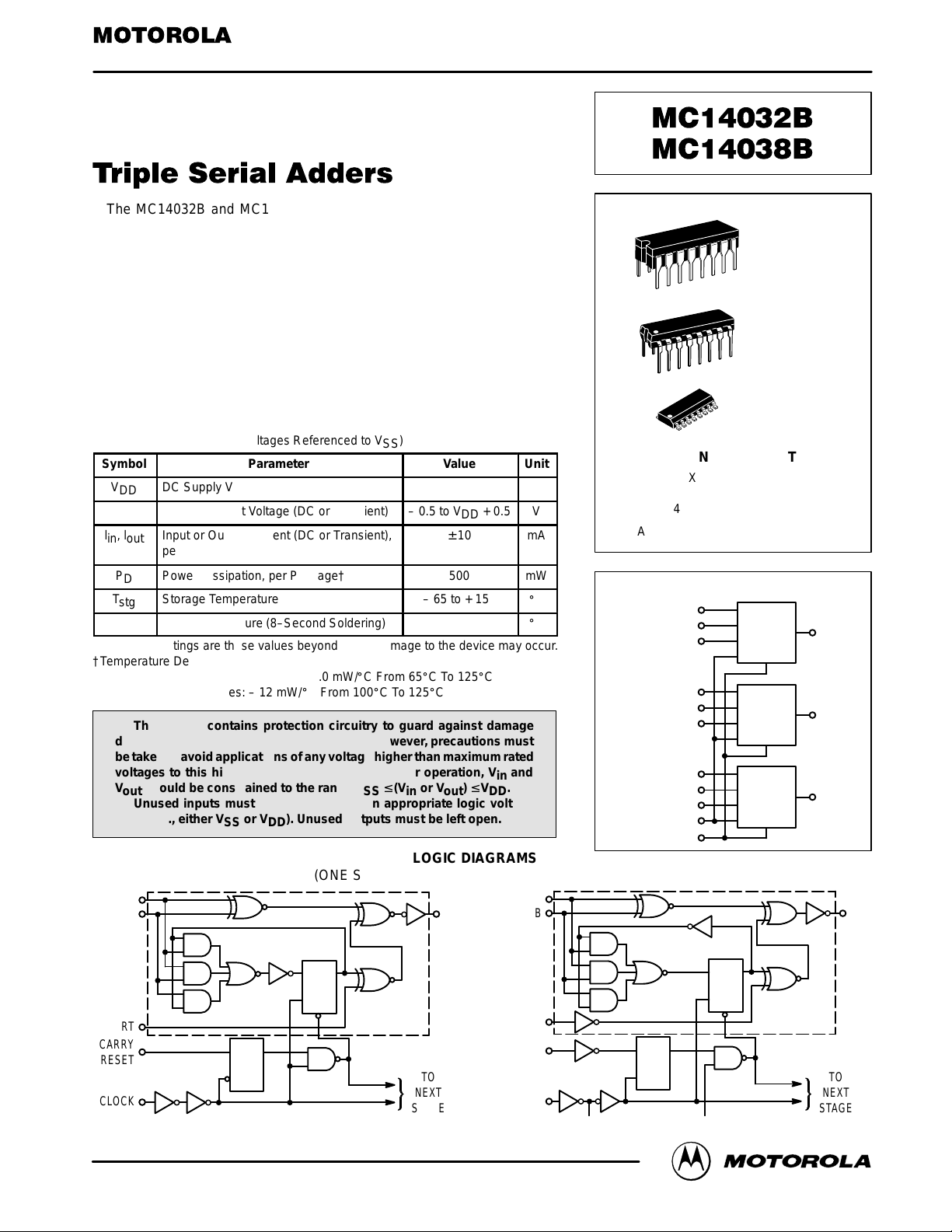
The MC14032B and MC14038B triple serial adders have the clock and
carry reset inputs common to all three adders. The carry is added on the
positive–going clock transition f or the MC14032B, and on the negative–
going clock transition for the MC14038B. Typical applications include serial
arithmetic units, digital correlators, digital servo control systems, datalink
computers, and flight control computers.
• Buffered Outputs
• Single–Phase Clocking
• Supply Voltage Range = 3.0 Vdc to 18 Vdc
• Capable of Driving Two Low–power TTL Loads or One Low–power
Schottky TTL Load Over the Rated Temperature Range.
• Pin–for–Pin Replacement for CD4032B and CD4038B.
MAXIMUM RATINGS* (Voltages Referenced to V
SS
)
Symbol
Parameter
Value
Unit
V
DD
DC Supply Voltage
– 0.5 to + 18.0
V
Vin, V
out
Input or Output Voltage (DC or Transient)
– 0.5 to VDD + 0.5
V
lin, l
out
Input or Output Current (DC or Transient),
per Pin
± 10
mA
P
D
Power Dissipation, per Package†
500
mW
T
stg
Storage Temperature
– 65 to + 150
_
C
T
L
Lead Temperature (8–Second Soldering)
260
_
C
*Maximum Ratings are those values beyond which damage to the device may occur.
†Temperature Derating:
Plastic “P and D/DW” Packages: – 7.0 mW/_C From 65_C To 125_C
Ceramic “L” Packages: – 12 mW/_C From 100_C To 125_C
This device contains protection circuitry to guard against damage
due to high static voltages or electric fields. However, precautions must
be taken to avoid applications of any voltage higher than maximum rated
voltages to this high-impedance circuit. For proper operation, Vin and
V
out
should be constrained to the range VSS ≤ (Vin or V
out
) ≤ VDD.
Unused inputs must always be tied to an appropriate logic voltage
level (e.g., either VSS or VDD). Unused outputs must be left open.
LOGIC DIAGRAMS
(ONE SECTION AND COMMON INPUTS SHOWN)
B
A
INVERT
CARRY
RESET
CLOCK
TO
NEXT
STAGE
TO
NEXT
STAGE
B
A
INVERT
CARRY
RESET
CLOCK
DRQ
C
D Q
C
S S
DRQ
C
D Q
C
MC14032B MC14038B
SEMICONDUCTOR TECHNICAL DATA
Motorola, Inc. 1995
REV 3
1/94
L SUFFIX
CERAMIC
CASE 620
ORDERING INFORMATION
MC14XXXBCP Plastic
MC14XXXBCL Ceramic
MC14XXXBD SOIC
TA = – 55° to 125°C for all packages.
P SUFFIX
PLASTIC
CASE 648
D SUFFIX
SOIC
CASE 751B
BLOCK DIAGRAM
CARRY RESET 6
CLOCK 3
INVERT 3 2
B3 14
A3 15
ADDER 3 1 S3
VDD = PIN 16
VSS = PIN 8
INVERT 2 5
B2 12
A2 13
ADDER 2 4 S2
INVERT 1 7
B1 11
A1 10
ADDER 1 9 S1
MOTOROLA CMOS LOGIC DATA
129
MC14032B MC14038B
ELECTRICAL CHARACTERISTICS (Voltages Referenced to V
SS
)
V
– 55_C
25_C
125_C
Characteristic
Symbol
V
DD
Vdc
Min
Max
Min
Typ #
Max
Min
ÎÎÎ
ÎÎÎ
ÎÎÎ
Max
Unit
“0” Level
Vin = VDD or 0
V
OL
5.0
10
15
—
—
—
0.05
0.05
0.05
—
—
—
0
0
0
0.05
0.05
0.05
—
—
—
ÎÎÎ
ÎÎÎ
ÎÎÎ
ÎÎÎ
0.05
0.05
0.05
Vdc
“1” Level
Vin = 0 or V
DD
V
OH
5.0
10
15
4.95
9.95
14.95
—
—
—
4.95
9.95
14.95
5.0
10
15
—
—
—
4.95
9.95
14.95
ÎÎÎ
ÎÎÎ
ÎÎÎ
ÎÎÎ
ÎÎÎ
—
—
—
Vdc
“0” Level
(VO = 4.5 or 0.5 Vdc)
(VO = 9.0 or 1.0 Vdc)
(VO = 13.5 or 1.5 Vdc)
V
IL
5.0
10
15
—
—
—
1.5
3.0
4.0
—
—
—
2.25
4.50
6.75
1.5
3.0
4.0
—
—
—
ÎÎÎ
ÎÎÎ
ÎÎÎ
ÎÎÎ
ÎÎÎ
1.5
3.0
4.0
Vdc
“1” Level
(VO = 0.5 or 4.5 Vdc)
(VO = 1.0 or 9.0 Vdc)
(VO = 1.5 or 13.5 Vdc)
V
IH
5.0
10
15
3.5
7.0
11
—
—
—
3.5
7.0
11
2.75
5.50
8.25
—
—
—
3.5
7.0
11
ÎÎÎ
ÎÎÎ
ÎÎÎ
ÎÎÎ
ÎÎÎ
—
—
—
Vdc
I
OH
5.0
5.0
10
15
– 3.0
– 0.64
– 1.6
– 4.2
—
—
—
—
– 2.4
– 0.51
– 1.3
– 3.4
– 4.2
– 0.88
– 2.25
– 8.8
—
—
—
—
– 1.7
– 0.36
– 0.9
– 2.4
ÎÎÎ
ÎÎÎ
ÎÎÎ
ÎÎÎ
ÎÎÎ
—
—
—
—
mAdc
I
OL
5.0
10
15
0.64
1.6
4.2
—
—
—
0.51
1.3
3.4
0.88
2.25
8.8
—
—
—
0.36
0.9
2.4
ÎÎÎ
ÎÎÎ
ÎÎÎ
ÎÎÎ
ÎÎÎ
—
—
—
mAdc
Input Current
I
in
15
—
± 0.1
—
±0.00001
± 0.1
—
ÎÎÎ
ÎÎÎ
ÎÎÎ
± 1.0
µAdc
Input Capacitance
(Vin = 0)
C
in
—
—
—
—
5.0
7.5
—
ÎÎÎ
ÎÎÎ
ÎÎÎ
—
pF
Quiescent Current
(Per Package)
I
DD
5.0
10
15
—
—
—
5.0
10
20
—
—
—
0.005
0.010
0.015
5.0
10
20
—
—
—
ÎÎÎ
ÎÎÎ
ÎÎÎ
ÎÎÎ
ÎÎÎ
150
300
600
µAdc
Total Supply Current**†
(Dynamic plus Quiescent,
Per Package)
(CL = 50 pF on all outputs, all
buffers switching)
I
T
5.0
10
15
IT = (0.96 µA/kHz) f + I
DD
IT = (1.93 µA/kHz) f + I
DD
IT = (2.80 µA/kHz) f + I
DD
µAdc
#Data labelled “Typ” is not to be used for design purposes but is intended as an indication of the IC’s potential performance.
**The formulas given are for the typical characteristics only at 25_C.
†To calculate total supply current at loads other than 50 pF:
IT(CL) = IT(50 pF) + (CL – 50) Vfk
where: IT is in µA (per package), CL in pF, V = (VDD – VSS) in volts, f in kHz is input frequency, and k = 0.003.
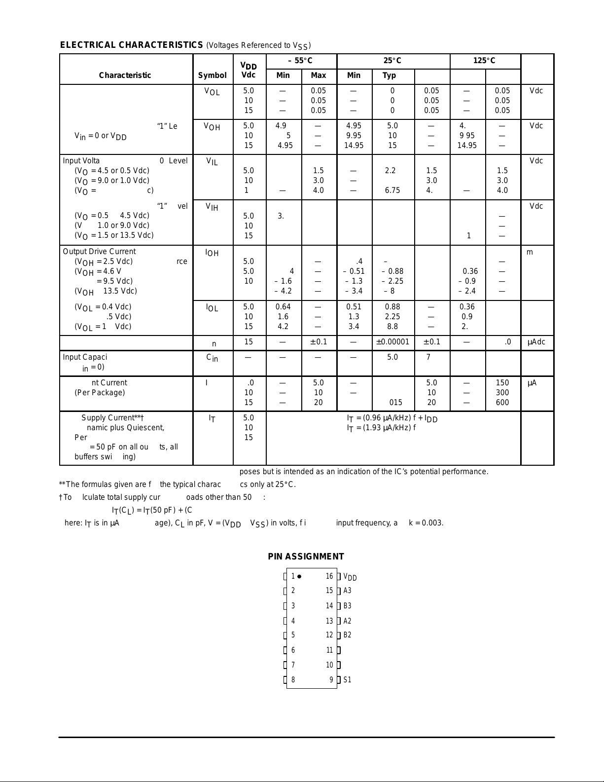
PIN ASSIGNMENT
13
14
15
16
9
10
11
125
4
3
2
1
8
7
6
B2
A2
B3
A3
V
DD
S1
A1
B1
S2
C
INV 3
S3
V
SS
INV 1
CARRY
RESET
INV 2
Output Voltage
Input Voltage
Output Drive Current
(VOH = 2.5 Vdc) Source
(VOH = 4.6 Vdc)
(VOH = 9.5 Vdc)
(VOH = 13.5 Vdc)
(VOL = 0.4 Vdc) Sink
(VOL = 0.5 Vdc)
(VOL = 1.5 Vdc)
MOTOROLA CMOS LOGIC DATAMC14032B MC14038B
130
SWITCHING CHARACTERISTICS* (C
L
= 50 pF, TA = 25_C)
Characteristic
ÎÎÎÎ
ÎÎÎÎ
ÎÎÎÎ
ÎÎÎÎ
Symbol
V
DD
Vdc
ÎÎÎÎ
ÎÎÎÎ
ÎÎÎÎ
ÎÎÎÎ
Min
Typ #
Max
Unit
Output Rise and Fall Time
t
TLH
, t
THL
= (1.5 ns/pF) CL + 25 ns
t
TLH
, t
THL
= (0.75 ns/pF) CL + 12.5 ns
t
TLH
, t
THL
= (0.55 ns/pF) CL + 9.5 ns
ÎÎÎÎ
ÎÎÎÎ
ÎÎÎÎ
ÎÎÎÎ
ÎÎÎÎ
t
TLH
,
t
THL
5.0
10
15
ÎÎÎÎ
ÎÎÎÎ
ÎÎÎÎ
ÎÎÎÎ
ÎÎÎÎ
—
—
—
100
50
40
200
100
80
ns
ÎÎÎÎ
ÎÎÎÎ
ÎÎÎÎ
ÎÎÎÎ
ÎÎÎÎ
5.0
10
15
ÎÎÎÎ
ÎÎÎÎ
ÎÎÎÎ
ÎÎÎÎ
ÎÎÎÎ
—
—
—
280
120
90
1400
300
230
ns
ÎÎÎÎ
ÎÎÎÎ
ÎÎÎÎ
ÎÎÎÎ
ÎÎÎÎ
5.0
10
15
ÎÎÎÎ
ÎÎÎÎ
ÎÎÎÎ
ÎÎÎÎ
ÎÎÎÎ
—
—
—
500
180
135
2400
600
450
ns
Input Setup Time
ÎÎÎÎ
ÎÎÎÎ
ÎÎÎÎ
ÎÎÎÎ
ÎÎÎÎ
t
su
5.0
10
15
ÎÎÎÎ
ÎÎÎÎ
ÎÎÎÎ
ÎÎÎÎ
ÎÎÎÎ
10
10
10
– 10
0
0
—
—
—
ns
Clock Pulse Frequency
ÎÎÎÎ
ÎÎÎÎ
ÎÎÎÎ
ÎÎÎÎ
f
cl
5.0
10
15
ÎÎÎÎ
ÎÎÎÎ
ÎÎÎÎ
ÎÎÎÎ
—
—
—
4.0
10
12
1.0
2.5
4.0
MHz
Clock Rise and Fall Times
ÎÎÎÎ
ÎÎÎÎ
ÎÎÎÎ
ÎÎÎÎ
t
THL
, t
TLH
5.0
10
15
ÎÎÎÎ
ÎÎÎÎ
ÎÎÎÎ
ÎÎÎÎ
—
—
—
—
—
—
1 5
5
4
µs
*The formulas given are for the typical characteristics only at 25_C.
#Data labelled “Typ” is not to be used for design purposes but is intended as an indication of the IC’s potential performance.
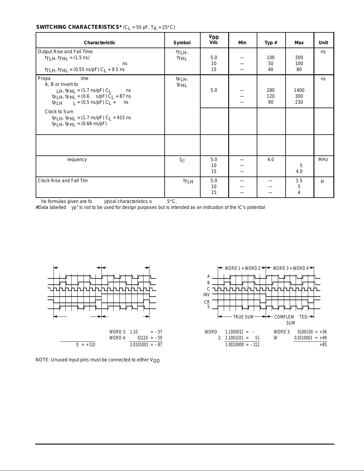
TIMING DIAGRAMS
MC14032B MC14038B
A
B
C
INV
CR
S
WORD 1 + WORD 2 WORD 3 + WORD 4
TRUE SUM COMPLEMENTED
SUM
WORD 1:
WORD 2:
0.0111100
0.0110010==
+60
+50
0.1101110 = +110
WORD 3:
WORD 4:
1.1011011
1.1001110==
–37
–50
1.0101001 = –87
WORD 1:
WORD 2:
1.1000011
1.1001101==
–61
–51
1.0010000 = –112
WORD 3:
WORD 4:
0.0100100
0.0110001==
+36
+49
0.1010101 = +85
TRUE SUM COMPLEMENTED
SUM
WORD 1 + WORD 2 WORD 3 + WORD 4
A
B
C
INV
CR
S
NOTE: Unused input pins must be connected to either VDD or VSS.
Propagation Delay Time
A, B or Invert to Sum
t
, t
PLH
t
PLH
t
PLH
= (1.7 ns/pF) CL + 195 ns
PHL
, t
= (0.66 ns/pF) CL + 87 ns
PHL
, t
= (0.5 ns/pF) CL + 65 ns
PHL
t
PLH
t
PHL
,
Clock to Sum
t
, t
PLH
t
PLH
t
PLH
= (1.7 ns/pF) CL + 415 ns
PHL
, t
= (0.66 ns/pF) CL + 147 ns
PHL
, t
= (0.5 ns/pF) CL + 110 ns
PHL
 Loading...