

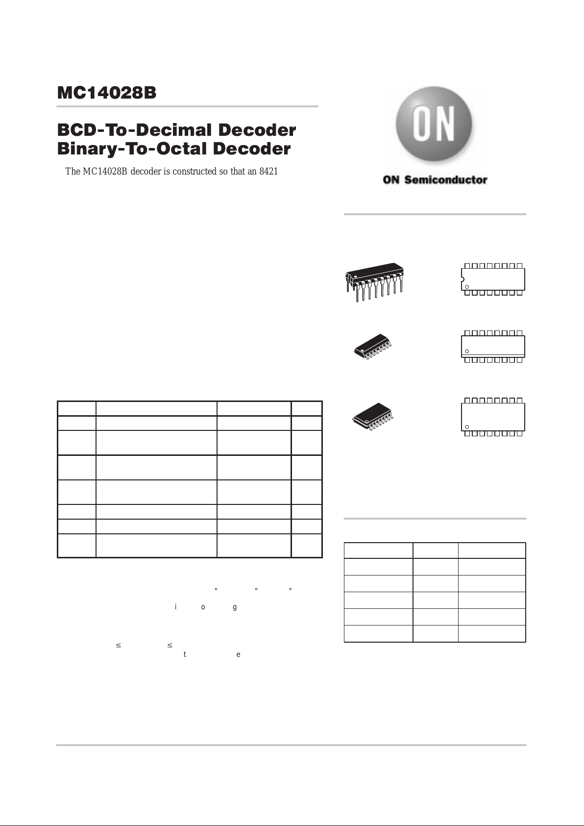
MOTOROLA MC14028BFEL, MC14028BFL1, MC14028BCP, MC14028BD, MC14028BDR2 Datasheet
...
Semiconductor Components Industries, LLC, 2000
March, 2000 – Rev. 3
1 Publication Order Number:
MC14028B/D
MC14028B
BCD-To-Decimal Decoder
Binary-To-Octal Decoder
The MC14028B decoder is constructed so that an 8421 BCD code
on the four inputs provides a decimal (one–of–ten) decoded output,
while a 3–bit binary input provides a decoded octal (one–of–eight)
code output with D forced to a logic “0”. Expanded decoding such as
binary–to–hexadecimal (one–of–16), etc., can be achieved by using
other MC14028B devices. The part is useful for code conversion,
address decoding, memory selection control, demultiplexing, or
readout decoding.
• Diode Protection on All Inputs
• Supply Voltage Range = 3.0 Vdc to 18 Vdc
• Capable of Driving Two Low–power TTL Loads or One Low–power
Schottky TTL Load Over the Rated Temperature Range
• Positive Logic Design
• Low Outputs on All Illegal Input Combinations
• Similar to CD4028B.
MAXIMUM RATINGS (Voltages Referenced to V
SS
) (Note 2.)
Symbol Parameter Value Unit
V
DD
DC Supply Voltage Range –0.5 to +18.0 V
Vin, V
out
Input or Output Voltage Range
(DC or Transient)
–0.5 to VDD + 0.5 V
Iin, I
out
Input or Output Current
(DC or Transient) per Pin
±10 mA
P
D
Power Dissipation,
per Package (Note 3.)
500 mW
T
A
Ambient Temperature Range –55 to +125 °C
T
stg
Storage Temperature Range –65 to +150 °C
T
L
Lead Temperature
(8–Second Soldering)
260 °C
2. Maximum Ratings are those values beyond which damage to the device
may occur.
3. Temperature Derating:
Plastic “P and D/DW” Packages: – 7.0 mW/_C From 65_C T o 125_C
This device contains protection circuitry to guard against damage due to high
static voltages or electric fields. However, precautions must be taken to avoid
applications of any voltage higher than maximum rated voltages to this
high–impedance circuit. For proper operation, V
in
and V
out
should be constrained
to the range V
SS
v (Vin or V
out
) v VDD.
Unused inputs must always be tied to an appropriate logic voltage level (e.g.,
either V
SS
or VDD). Unused outputs must be left open.
http://onsemi.com
A = Assembly Location
WL or L = Wafer Lot
YY or Y = Year
WW or W = Work Week
Device Package Shipping
ORDERING INFORMATION
MC14028BCP PDIP–16 2000/Box
MC14028BD SOIC–16 2400/Box
MC14028BDR2 SOIC–16 2500/Tape & Reel
1. For ordering information on the EIAJ version of
the SOIC packages, please contact your local
ON Semiconductor representative.
MARKING
DIAGRAMS
1
16
PDIP–16
P SUFFIX
CASE 648
MC14028BCP
AWLYYWW
SOIC–16
D SUFFIX
CASE 751B
1
16
14028B
AWLYWW
SOEIAJ–16
F SUFFIX
CASE 966
1
16
MC14028B
AWLYWW
MC14028BF SOEIAJ–16 See Note 1.
MC14028BFEL SOEIAJ–16 See Note 1.
MC14028B
http://onsemi.com
2
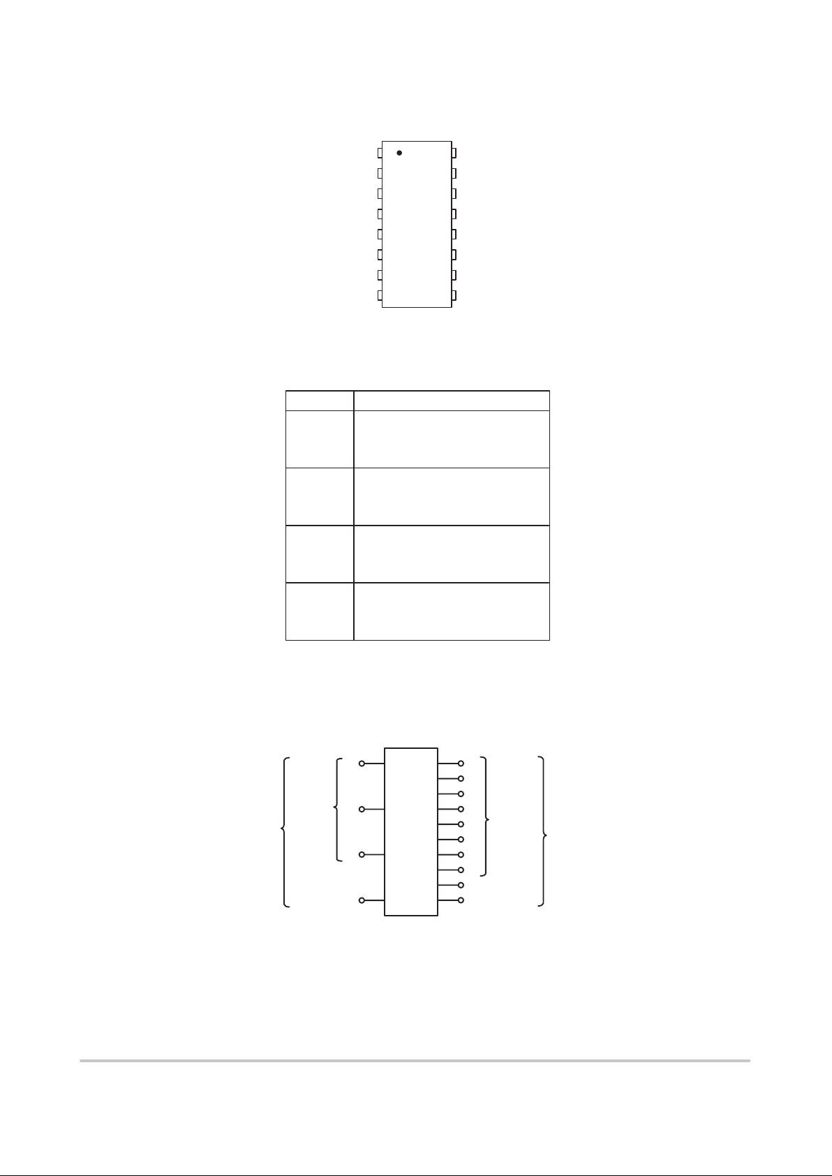
PIN ASSIGNMENT
13
14
15
16
9
10
11
125
4
3
2
1
8
7
6
C
B
Q1
Q3
V
DD
Q8
A
D
Q7
Q0
Q2
Q4
V
SS
Q6
Q5
Q9
TRUTH TABLE
DC B A Q9Q8Q7Q6Q5Q4Q3Q2Q1Q0
00000000000001
00010000000010
00100000000100
00110000001000
01000000010000
01010000100000
01100001000000
01110010000000
10000100000000
10011000000000
10100000000000
10110000000000
11000000000000
11010000000000
11100000000000
11110000000000
BLOCK DIAGRAM
8421
BCD
INPUTS
DECIMAL
DECODED
OUTPUTS
OCTAL
DECODED
OUTPUTS
3
14
2
15
1
6
7
4
9
5
A
B
C
DQ9
Q8
Q7
Q6
Q5
Q4
Q3
Q2
Q1
Q0
3–BIT
BINARY
INPUTS
10
13
12
11
V
DD
= PIN 16
V
SS
= PIN 8
MC14028B
http://onsemi.com
3
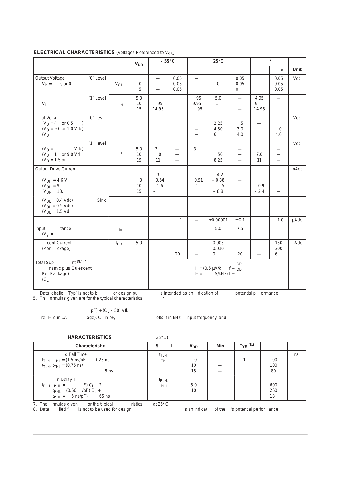
ELECTRICAL CHARACTERISTICS (Voltages Referenced to V
SS
)
V
– 55_C
25_C
125_C
Characteristic
Symbol
V
DD
Vdc
Min
Max
Min
Typ
(4.)
Max
Min
Max
Unit
ОООООООО
Î
Output Voltage “0” Level
V
in
= VDD or 0
ÎÎ
Î
V
OL
Î
Î
5.0
10
15
Î
Î
—
—
—
Î
Î
0.05
0.05
0.05
ÎÎ
Î
—
—
—
Î
Î
0
0
0
ÎÎ
Î
0.05
0.05
0.05
Î
Î
—
—
—
Î
Î
0.05
0.05
0.05
Î
Î
Vdc
ОООООООО
Î
“1” Level
V
in
= 0 or V
DD
ÎÎ
Î
V
OH
Î
Î
5.0
10
15
Î
Î
4.95
9.95
14.95
Î
Î
—
—
—
ÎÎ
Î
4.95
9.95
14.95
Î
Î
5.0
10
15
ÎÎ
Î
—
—
—
Î
Î
4.95
9.95
14.95
Î
Î
—
—
—
Î
Î
Vdc
ОООООООО
Î
ОООООООО
Î
Input Voltage “0” Level
(V
O
= 4.5 or 0.5 Vdc)
(V
O
= 9.0 or 1.0 Vdc)
(V
O
= 13.5 or 1.5 Vdc)
ÎÎ
Î
ÎÎ
Î
V
IL
Î
Î
Î
Î
5.0
10
15
Î
Î
Î
Î
—
—
—
Î
Î
Î
Î
1.5
3.0
4.0
ÎÎ
Î
ÎÎ
Î
—
—
—
Î
Î
Î
Î
2.25
4.50
6.75
ÎÎ
Î
ÎÎ
Î
1.5
3.0
4.0
Î
Î
Î
Î
—
—
—
Î
Î
Î
Î
1.5
3.0
4.0
Î
Î
Î
Î
Vdc
ОООООООО
Î
ОООООООО
Î
“1” Level
(V
O
= 0.5 or 4.5 Vdc)
(V
O
= 1.0 or 9.0 Vdc)
(V
O
= 1.5 or 13.5 Vdc)
ÎÎ
Î
ÎÎ
Î
V
IH
Î
Î
Î
Î
5.0
10
15
Î
Î
Î
Î
3.5
7.0
11
Î
Î
Î
Î
—
—
—
ÎÎ
Î
ÎÎ
Î
3.5
7.0
11
Î
Î
Î
Î
2.75
5.50
8.25
ÎÎ
Î
ÎÎ
Î
—
—
—
Î
Î
Î
Î
3.5
7.0
11
Î
Î
Î
Î
—
—
—
Î
Î
Î
Î
Vdc
ОООООООО
Î
ОООООООО
Î
ОООООООО
Î
Output Drive Current
(V
OH
= 2.5 Vdc) Source
(V
OH
= 4.6 Vdc)
(V
OH
= 9.5 Vdc)
(V
OH
= 13.5 Vdc)
ÎÎ
Î
ÎÎ
Î
ÎÎ
Î
I
OH
Î
Î
Î
Î
Î
Î
5.0
5.0
10
15
Î
Î
Î
Î
Î
Î
– 3.0
– 0.64
– 1.6
– 4.2
Î
Î
Î
Î
Î
Î
—
—
—
—
ÎÎ
Î
ÎÎ
Î
ÎÎ
Î
– 2.4
– 0.51
– 1.3
– 3.4
Î
Î
Î
Î
Î
Î
– 4.2
– 0.88
– 2.25
– 8.8
ÎÎ
Î
ÎÎ
Î
ÎÎ
Î
—
—
—
—
Î
Î
Î
Î
Î
Î
– 1.7
– 0.36
– 0.9
– 2.4
Î
Î
Î
Î
Î
Î
—
—
—
—
Î
Î
Î
Î
Î
Î
mAdc
ОООООООО
Î
(VOL = 0.4 Vdc) Sink
(V
OL
= 0.5 Vdc)
(V
OL
= 1.5 Vdc)
ÎÎ
Î
I
OL
Î
Î
5.0
10
15
Î
Î
0.64
1.6
4.2
Î
Î
—
—
—
ÎÎ
Î
0.51
1.3
3.4
Î
Î
0.88
2.25
8.8
ÎÎ
Î
—
—
—
Î
Î
0.36
0.9
2.4
Î
Î
—
—
—
Î
Î
mAdc
Input Current
I
in
15
—
± 0.1
—
±0.00001
± 0.1
—
± 1.0
µAdc
ОООООООО
Î
Input Capacitance
(V
in
= 0)
ÎÎ
Î
C
in
Î
Î
—
Î
Î
—
Î
Î
—
ÎÎ
Î
—
Î
Î
5.0
ÎÎ
Î
7.5
Î
Î
—
Î
Î
—
Î
Î
pF
ОООООООО
Î
Quiescent Current
(Per Package)
ÎÎ
Î
I
DD
Î
Î
5.0
10
15
Î
Î
—
—
—
Î
Î
5.0
10
20
ÎÎ
Î
—
—
—
Î
Î
0.005
0.010
0.015
ÎÎ
Î
5.0
10
20
Î
Î
—
—
—
Î
Î
150
300
600
Î
Î
µAdc
ОООООООО
Î
ОООООООО
Î
ОООООООО
Î
Total Supply Current
(5.) (6.)
(Dynamic plus Quiescent,
Per Package)
(C
L
= 50 pF on all outputs, all
buffers switching)
ÎÎ
Î
ÎÎ
Î
ÎÎ
Î
I
T
Î
Î
Î
Î
Î
Î
5.0
10
15
ООООООООООООООО
Î
ООООООООООООООО
Î
ООООООООООООООО
Î
IT = (0.3 µA/kHz) f + I
DD
IT = (0.6 µA/kHz) f + I
DD
IT = (0.9 µA/kHz) f + I
DD
Î
Î
Î
Î
Î
Î
µAdc
4. Data labelled “Typ” is not to be used for design purposes but is intended as an indication of the IC’s potential performance.
5. The formulas given are for the typical characteristics only at 25_C.
6. To calculate total supply current at loads other than 50 pF:
I
T(CL
) = IT(50 pF) + (CL – 50) Vfk
where: I
T
is in µA (per package), CL in pF, V = (VDD – VSS) in volts, f in kHz is input frequency, and k = 0.001.
SWITCHING CHARACTERISTICS
(7.)
(C
L
= 50 pF, T
A
= 25_C)
Characteristic
Symbol
V
DD
Min
Typ
(8.)
Max
Unit
ООООООООООООО
Î
ООООООООООООО
Î
Output Rise and Fall Time
t
TLH
, t
THL
= (1.5 ns/pF) CL + 25 ns
t
TLH
, t
THL
= (0.75 ns/pF) CL + 12.5 ns
t
TLH
, t
THL
= (0.55 ns/pF) CL + 9.5 ns
ÎÎÎ
Î
ÎÎÎ
Î
t
TLH
,
t
THL
ÎÎ
Î
ÎÎ
Î
5.0
10
15
ÎÎ
Î
ÎÎ
Î
—
—
—
ÎÎ
Î
ÎÎ
Î
100
50
40
ÎÎ
Î
ÎÎ
Î
200
100
80
Î
Î
Î
Î
ns
ООООООООООООО
Î
ООООООООООООО
Î
Propagation Delay Time
t
PLH
, t
PHL
= (1.7 ns/pF) CL + 215 ns
t
PLH
, t
PHL
= (0.66 ns/pF) CL + 97 ns
t
PLH
, t
PHL
= (0.5 ns/pF) CL + 65 ns
ÎÎÎ
Î
ÎÎÎ
Î
t
PLH
,
t
PHL
ÎÎ
Î
ÎÎ
Î
5.0
10
15
ÎÎ
Î
ÎÎ
Î
—
—
—
ÎÎ
Î
ÎÎ
Î
300
130
90
ÎÎ
Î
ÎÎ
Î
600
260
180
Î
Î
Î
Î
ns
7. The formulas given are for the typical characteristics only at 25_C.
8. Data labelled “Typ” is not to be used for design purposes but is intended as an indication of the IC’s potential performance.
 Loading...