

Motorola MC14028BD, MC14028BCL, MC14028BCP Datasheet
MOTOROLA CMOS LOGIC DATA
113
MC14028B
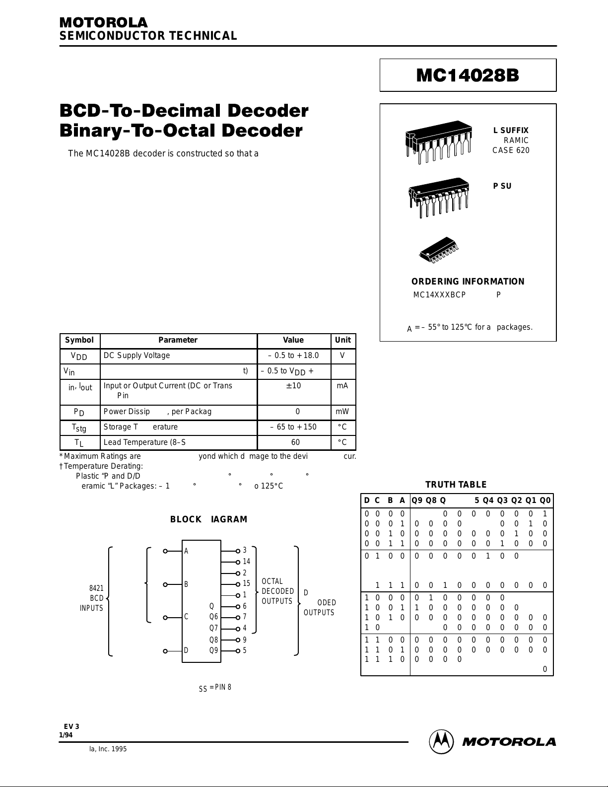
The MC14028B decoder is constructed so that an 8421 BCD code on the
four inputs provides a decimal (one–of–ten) decoded output, while a 3–bit
binary input provides a decoded octal (one–of–eight) code output with D
forced to a logic “0”. Expanded decoding such as binary–to–hexadecimal
(one–of–16), etc., can be achieved by using other MC14028B devices. The
part is useful for code conversion, address decoding, memory selection
control, demultiplexing, or readout decoding.
• Diode Protection on All Inputs
• Supply Voltage Range = 3.0 Vdc to 18 Vdc
• Capable of Driving Two Low–power TTL Loads or One Low–power
Schottky TTL Load Over the Rated Temperature Range
• Positive Logic Design
• Low Outputs on All Illegal Input Combinations
• Similar to CD4028B.
MAXIMUM RATINGS* (Voltages Referenced to V
SS
)
Symbol
Parameter
Value
Unit
V
DD
DC Supply Voltage
– 0.5 to + 18.0
V
Vin, V
out
Input or Output Voltage (DC or Transient)
– 0.5 to VDD + 0.5
V
lin, l
out
Input or Output Current (DC or Transient),
per Pin
± 10
mA
P
D
Power Dissipation, per Package†
500
mW
T
stg
Storage Temperature
– 65 to + 150
_
C
T
L
Lead Temperature (8–Second Soldering)
260
_
C
*Maximum Ratings are those values beyond which damage to the device may occur.
†Temperature Derating:
Plastic “P and D/DW” Packages: – 7.0 mW/_C From 65_C To 125_C
Ceramic “L” Packages: – 12 mW/_C From 100_C To 125_C
BLOCK DIAGRAM
8421
BCD
INPUTS
DECIMAL
DECODED
OUTPUTS
OCTAL
DECODED
OUTPUTS
3
14
2
15
1
6
7
4
9
5
A
B
C
D Q9
Q8
Q7
Q6
Q5
Q4
Q3
Q2
Q1
Q0
3–BIT
BINARY
INPUTS
10
13
12
11
VDD = PIN 16
VSS = PIN 8
TRUTH TABLE
D C B A Q9 Q8 Q7 Q6 Q5 Q4 Q3 Q2 Q1 Q0
0 0 0 0 0 0 0 0 0 0 0 0 0 1
0 0 0 1 0 0 0 0 0 0 0 0 1 0
0 0 1 0 0 0 0 0 0 0 0 1 0 0
0 0 1 1 0 0 0 0 0 0 1 0 0 0
0 1 0 0 0 0 0 0 0 1 0 0 0 0
0 1 0 1 0 0 0 0 1 0 0 0 0 0
0 1 1 0 0 0 0 1 0 0 0 0 0 0
0 1 1 1 0 0 1 0 0 0 0 0 0 0
1 0 0 0 0 1 0 0 0 0 0 0 0 0
1 0 0 1 1 0 0 0 0 0 0 0 0 0
1 0 1 0 0 0 0 0 0 0 0 0 0 0
1 0 1 1 0 0 0 0 0 0 0 0 0 0
1 1 0 0 0 0 0 0 0 0 0 0 0 0
1 1 0 1 0 0 0 0 0 0 0 0 0 0
1 1 1 0 0 0 0 0 0 0 0 0 0 0
1 1 1 1 0 0 0 0 0 0 0 0 0 0
SEMICONDUCTOR TECHNICAL DATA
Motorola, Inc. 1995
REV 3
1/94
L SUFFIX
CERAMIC
CASE 620
ORDERING INFORMATION
MC14XXXBCP Plastic
MC14XXXBCL Ceramic
MC14XXXBD SOIC
TA = – 55° to 125°C for all packages.
P SUFFIX
PLASTIC
CASE 648
D SUFFIX
SOIC
CASE 751B
MOTOROLA CMOS LOGIC DATAMC14028B
114
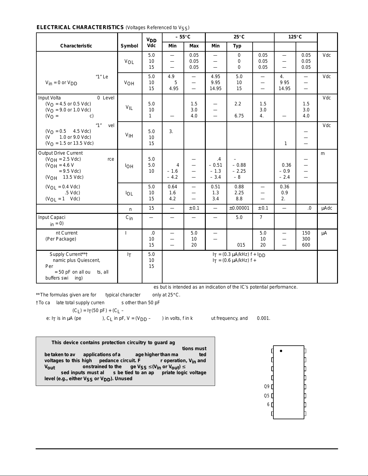
ELECTRICAL CHARACTERISTICS (Voltages Referenced to V
SS
)
V
– 55_C
25_C
125_C
Characteristic
Symbol
V
DD
Vdc
Min
Max
Min
Typ #
Max
Min
ÎÎÎ
ÎÎÎ
ÎÎÎ
Max
Unit
“0” Level
Vin = VDD or 0
V
OL
5.0
10
15
—
—
—
0.05
0.05
0.05
—
—
—
0
0
0
0.05
0.05
0.05
—
—
—
ÎÎÎ
ÎÎÎ
ÎÎÎ
ÎÎÎ
0.05
0.05
0.05
Vdc
“1” Level
Vin = 0 or V
DD
V
OH
5.0
10
15
4.95
9.95
14.95
—
—
—
4.95
9.95
14.95
5.0
10
15
—
—
—
4.95
9.95
14.95
ÎÎÎ
ÎÎÎ
ÎÎÎ
ÎÎÎ
ÎÎÎ
—
—
—
Vdc
“0” Level
(VO = 4.5 or 0.5 Vdc)
(VO = 9.0 or 1.0 Vdc)
(VO = 13.5 or 1.5 Vdc)
V
IL
5.0
10
15
—
—
—
1.5
3.0
4.0
—
—
—
2.25
4.50
6.75
1.5
3.0
4.0
—
—
—
ÎÎÎ
ÎÎÎ
ÎÎÎ
ÎÎÎ
ÎÎÎ
1.5
3.0
4.0
Vdc
“1” Level
(VO = 0.5 or 4.5 Vdc)
(VO = 1.0 or 9.0 Vdc)
(VO = 1.5 or 13.5 Vdc)
V
IH
5.0
10
15
3.5
7.0
11
—
—
—
3.5
7.0
11
2.75
5.50
8.25
—
—
—
3.5
7.0
11
ÎÎÎ
ÎÎÎ
ÎÎÎ
ÎÎÎ
ÎÎÎ
—
—
—
Vdc
I
OH
5.0
5.0
10
15
– 3.0
– 0.64
– 1.6
– 4.2
—
—
—
—
– 2.4
– 0.51
– 1.3
– 3.4
– 4.2
– 0.88
– 2.25
– 8.8
—
—
—
—
– 1.7
– 0.36
– 0.9
– 2.4
ÎÎÎ
ÎÎÎ
ÎÎÎ
ÎÎÎ
ÎÎÎ
—
—
—
—
mAdc
I
OL
5.0
10
15
0.64
1.6
4.2
—
—
—
0.51
1.3
3.4
0.88
2.25
8.8
—
—
—
0.36
0.9
2.4
ÎÎÎ
ÎÎÎ
ÎÎÎ
ÎÎÎ
ÎÎÎ
—
—
—
mAdc
Input Current
I
in
15
—
± 0.1
—
±0.00001
± 0.1
—
ÎÎÎ
ÎÎÎ
ÎÎÎ
± 1.0
µAdc
Input Capacitance
(Vin = 0)
C
in
—
—
—
—
5.0
7.5
—
ÎÎÎ
ÎÎÎ
ÎÎÎ
—
pF
Quiescent Current
(Per Package)
I
DD
5.0
10
15
—
—
—
5.0
10
20
—
—
—
0.005
0.010
0.015
5.0
10
20
—
—
—
ÎÎÎ
ÎÎÎ
ÎÎÎ
ÎÎÎ
ÎÎÎ
150
300
600
µAdc
Total Supply Current**†
(Dynamic plus Quiescent,
Per Package)
(CL = 50 pF on all outputs, all
buffers switching)
I
T
5.0
10
15
IT = (0.3 µA/kHz) f + I
DD
IT = (0.6 µA/kHz) f + I
DD
IT = (0.9 µA/kHz) f + I
DD
µAdc
#Data labelled “Typ” is not to be used for design purposes but is intended as an indication of the IC’s potential performance.
**The formulas given are for the typical characteristics only at 25_C.
†To calculate total supply current at loads other than 50 pF:
IT(CL) = IT(50 pF) + (CL – 50) Vfk
where: IT is in µA (per package), CL in pF, V = (VDD – VSS) in volts, f in kHz is input frequency, and k = 0.001.
This device contains protection circuitry to guard against damage
due to high static voltages or electric fields. However, precautions must
be taken to avoid applications of any voltage higher than maximum rated
voltages to this high-impedance circuit. For proper operation, Vin and
V
out
should be constrained to the range VSS ≤ (Vin or V
out
) ≤ VDD.
Unused inputs must always be tied to an appropriate logic voltage
level (e.g., either VSS or VDD). Unused outputs must be left open.
PIN ASSIGNMENT
13
14
15
16
9
10
11
125
4
3
2
1
8
7
6
C
B
Q1
Q3
V
DD
Q8
A
D
Q7
Q0
Q2
Q4
V
SS
Q6
Q5
Q9
Output Voltage
Input Voltage
Output Drive Current
(VOH = 2.5 Vdc) Source
(VOH = 4.6 Vdc)
(VOH = 9.5 Vdc)
(VOH = 13.5 Vdc)
(VOL = 0.4 Vdc) Sink
(VOL = 0.5 Vdc)
(VOL = 1.5 Vdc)
MOTOROLA CMOS LOGIC DATA
115
MC14028B
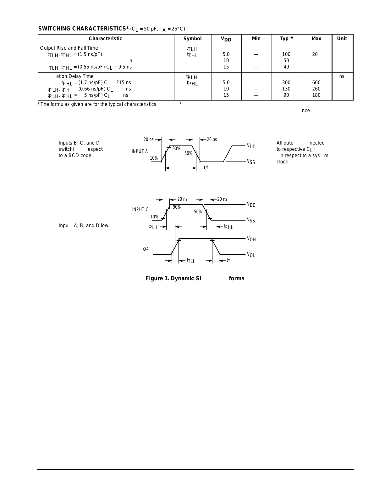
SWITCHING CHARACTERISTICS* (C
L
= 50 pF, TA = 25_C)
Characteristic
ÎÎÎÎ
ÎÎÎÎ
ÎÎÎÎ
Symbol
V
DD
ÎÎÎÎ
ÎÎÎÎ
ÎÎÎÎ
Min
Typ #
Max
Unit
Output Rise and Fall Time
t
TLH
, t
THL
= (1.5 ns/pF) CL + 25 ns
t
TLH
, t
THL
= (0.75 ns/pF) CL + 12.5 ns
t
TLH
, t
THL
= (0.55 ns/pF) CL + 9.5 ns
ÎÎÎÎ
ÎÎÎÎ
ÎÎÎÎ
ÎÎÎÎ
ÎÎÎÎ
t
TLH
,
t
THL
5.0
10
15
ÎÎÎÎ
ÎÎÎÎ
ÎÎÎÎ
ÎÎÎÎ
ÎÎÎÎ
—
—
—
100
50
40
200
100
80
ns
Propagation Delay Time
t
PLH
, t
PHL
= (1.7 ns/pF) CL + 215 ns
t
PLH
, t
PHL
= (0.66 ns/pF) CL + 97 ns
t
PLH
, t
PHL
= (0.5 ns/pF) CL + 65 ns
ÎÎÎÎ
ÎÎÎÎ
ÎÎÎÎ
ÎÎÎÎ
ÎÎÎÎ
t
PLH
,
t
PHL
5.0
10
15
ÎÎÎÎ
ÎÎÎÎ
ÎÎÎÎ
ÎÎÎÎ
ÎÎÎÎ
—
—
—
300
130
90
600
260
180
ns
*The formulas given are for the typical characteristics only at 25_C.
#Data labelled “Typ” is not to be used for design purposes but is intended as an indication of the IC’s potential performance.
Figure 1. Dynamic Signal Waveforms
Inputs B, C, and D
switching in respect
to a BCD code.
Inputs A, B, and D low.
All outputs connected
to respective CL loads.
f in respect to a system
clock.
20 ns 20 ns
90%
50%
10%
1/f
V
DD
V
SS
20 ns 20 ns
INPUT A
INPUT C
Q4
10%
90%
50%
V
DD
V
SS
V
OH
V
OL
t
PLH
t
PHL
t
TLH
t
THL
50%
90%
10%
 Loading...