

MOTOROLA MC14001UBCP, MC14001UBD, MC14001UBDR2 Datasheet
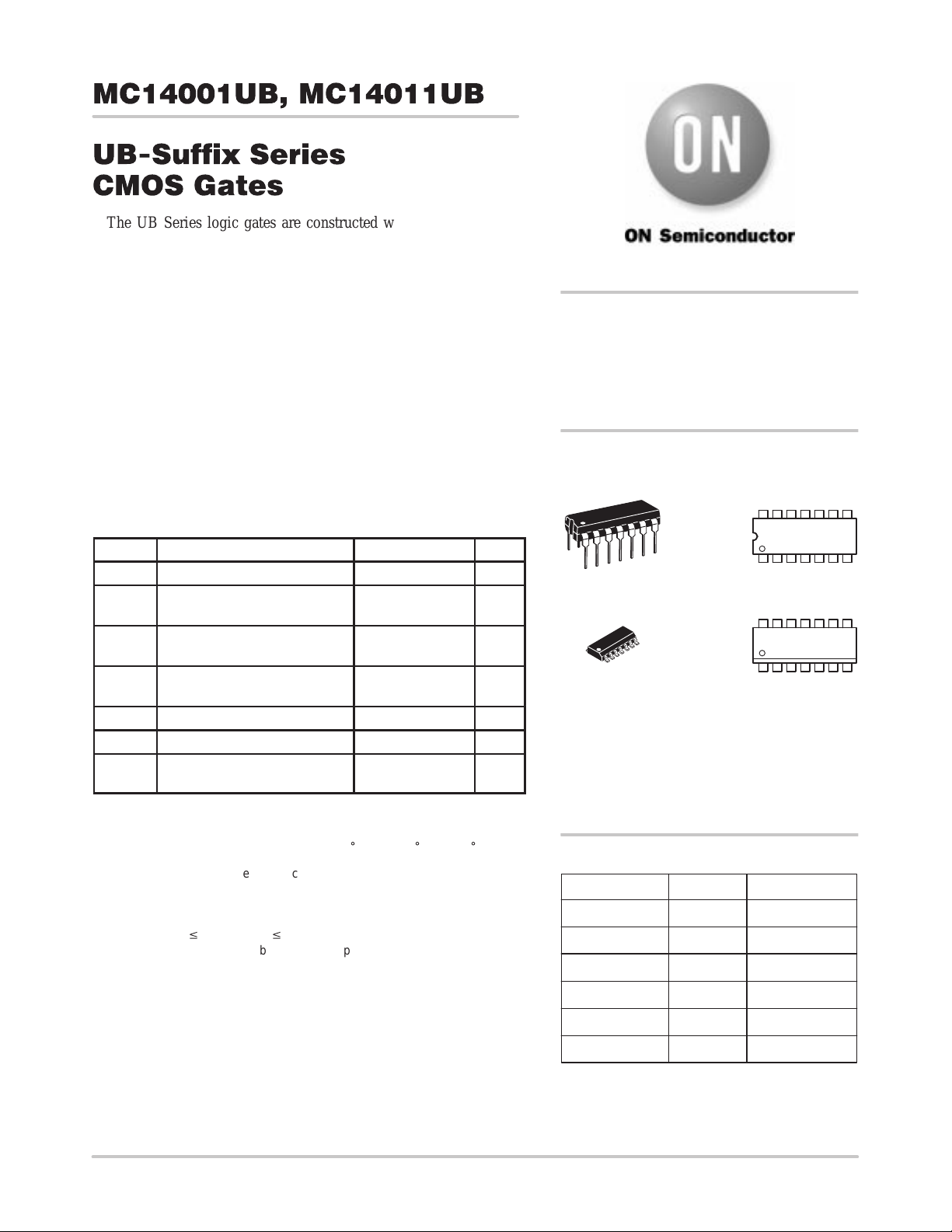
MC14001UB, MC14011UB
UB-Suffix Series
CMOS Gates
The UB Series logic gates are constructed with P and N channel
enhancement mode devices in a single monolithic structure
(Complementary MOS). Their primary use is where low power
dissipation and/or high noise immunity is desired. The UB set of
CMOS gates are inverting non–buffered functions.
• Supply Voltage Range = 3.0 Vdc to 18 Vdc
• Linear and Oscillator Applications
• Capable of Driving T wo Low–power TTL Loads or One Low–power
Schottky TTL Load Over the Rated T emperature Range
• Double Diode Protection on All Inputs
• Pin–for–Pin Replacements for Corresponding CD4000 Series UB
Suffix Devices
MAXIMUM RATINGS (Voltages Referenced to V
Symbol
V
DD
Vin, V
Iin, I
P
T
T
stg
T
1. Maximum Ratings are those values beyond which damage to the device
may occur.
2. Temperature Derating:
Plastic “P and D/DW” Packages: – 7.0 mW/_C From 65_C To 125_C
This device contains protection circuitry to guard against damage due to high
static voltages or electric fields. However, precautions must be taken to avoid
applications of any voltage higher than maximum rated voltages to this
high–impedance circuit. For proper operation, Vin and V
to the range V
Unused inputs must always be tied to an appropriate logic voltage level (e.g.,
either V
DC Supply Voltage Range –0.5 to +18.0 V
Input or Output Voltage Range
out
Input or Output Current
out
Power Dissipation,
D
Ambient Temperature Range –55 to +125 °C
A
Storage Temperature Range –65 to +150 °C
Lead Temperature
L
SS
or VDD). Unused outputs must be left open.
SS
Parameter Value Unit
(DC or Transient)
(DC or Transient) per Pin
per Package (Note 2.)
(8–Second Soldering)
v (Vin or V
) v VDD.
out
) (Note 1.)
SS
–0.5 to VDD + 0.5 V
±10 mA
500 mW
260 °C
should be constrained
out
http://onsemi.com
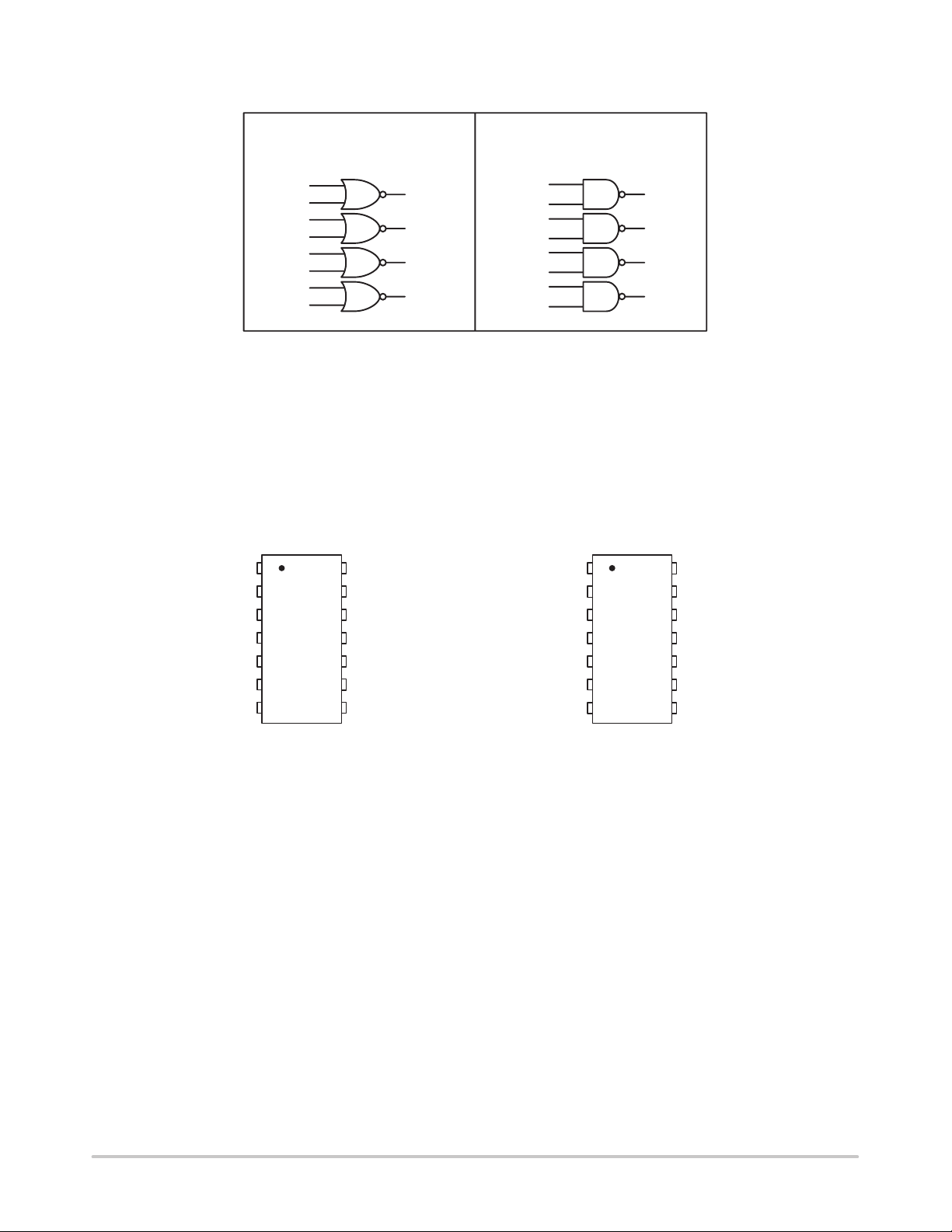
MC14001UB
Quad 2–Input NOR Gate
MC14011UB
Quad 2–Input NAND Gate
MARKING
DIAGRAMS
14
PDIP–14
P SUFFIX
CASE 646
SOIC–14
D SUFFIX
CASE 751A
XX = Specific Device Code
A = Assembly Location
WL or L = Wafer Lot
YY or Y = Year
WW or W = Work Week
ORDERING INFORMATION
Device Package Shipping
MC14001UBCP PDIP–14 2000/Box
MC14001UBD SOIC–14
MC14001UBDR2 SOIC–14 2500/Tape & Reel
MC1401 1UBCP PDIP–14
MC1401 1UBD SOIC–14
MC1401 1UBDR2 SOIC–14
MC140XXUBCP
AWLYYWW
1
14
140XXU
AWLYWW
1
55/Rail
2000/Box
55/Rail
2500/Tape & Reel
Semiconductor Components Industries, LLC, 2000
March, 2000 – Rev . 3
1 Publication Order Number:
MC14001UB/D
MC14001UB, MC14011UB
LOGIC DIAGRAMS
MC14001UB
Quad 2–Input
NOR Gate
1
2
5
6
8
9
12
13
MC14001UB
Quad 2–Input NOR Gate
IN 1
IN 2
OUT
OUT
IN 1
IN 2
1
A
2
A
3
A
4
B
B
6
B
7
V
SS
14
V
DD
13
IN 2
12
IN 1
11
OUT
OUT
105
9
IN 2
8
IN 1
3
4
10
11
VDD = PIN 14
V
= PIN 7
SS
FOR ALL DEVICES
PIN ASSIGNMENTS
D
D
D
C
C
C
MC14011UB
Quad 2–Input
NAND Gate
1
2
5
6
8
9
12
13
3
4
10
11
MC14011UB
Quad 2–Input NAND Gate
1
IN 1
IN 2
OUT
OUT
IN 1
IN 2
A
2
A
3
A
4
B
B
6
B
7
V
SS
14
13
12
11
105
9
8
V
DD
IN 2
IN 1
OUT
OUT
IN 2
IN 1
D
D
D
C
C
C
http://onsemi.com
2
MC14001UB, MC14011UB
V
DD
Î
Î
Î
Î
Î
Î
Î
Î
Î
Î
Î
Î
Î
Î
Î
Î
Î
Î
Î
Î
Î
Î
Î
Î
Î
Î
Î
Î
Î
Î
Î
Î
Î
Î
Î
Î
Î
Î
Î
Î
Î
Î
Î
Î
Î
Î
Î
Î
Î
Î
Î
Î
Î
Î
Î
Î
Î
Î
Î
Î
Î
Î
Î
Î
Î
Î
Î
Î
Î
Î
Î
Î
Î
Î
Î
Î
Î
Î
Î
Î
Î
Î
Î
Î
Î
Î
Î
Î
Î
Î
Î
Î
Î
Î
Î
Î
Î
Î
Î
Î
Î
Î
Î
Î
Î
Î
Î
Î
Î
Î
Î
Î
Î
Î
Î
Î
Î
Î
Î
Î
Î
Î
Î
Î
Î
Î
Î
Î
Î
Î
Î
Î
Î
Î
Î
Î
Î
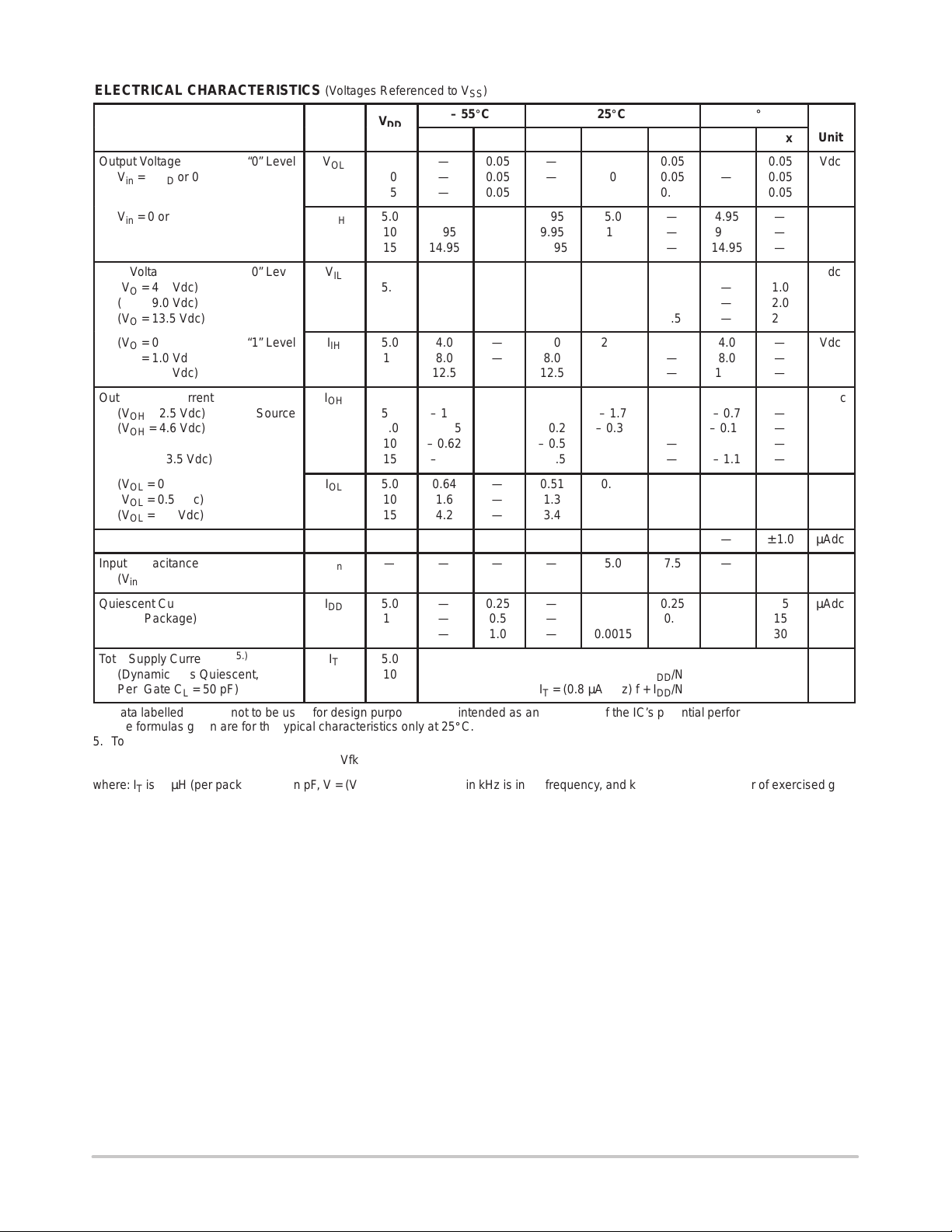
ELECTRICAL CHARACTERISTICS (Voltages Referenced to V
V
Characteristic
Output Voltage “0” Level
V
= VDD or 0
in
ОООООООО
Vin = 0 or V
ОООООООО
Input Voltage “0” Level
ОООООООО
(V
O
(V
ОООООООО
O
(V
O
(VO = 0.5 Vdc) “1” Level
ОООООООО
(V
O
(V
O
ОООООООО
DD
= 4.5 Vdc)
= 9.0 Vdc)
= 13.5 Vdc)
= 1.0 Vdc)
= 1.5 Vdc)
“1” Level
Output Drive Current
(V
= 2.5 Vdc) Source
OH
ОООООООО
(V
= 4.6 Vdc)
OH
(V
= 9.5 Vdc)
OH
ОООООООО
(V
= 13.5 Vdc)
OH
(VOL = 0.4 Vdc) Sink
ОООООООО
(V
= 0.5 Vdc)
OL
= 1.5 Vdc)
(V
OL
ОООООООО
Input Current
Input Capacitance
(V
= 0)
in
Quiescent Current
ОООООООО
(Per Package)
ОООООООО
Total Supply Current
(4.) (5.)
(Dynamic plus Quiescent,
ОООООООО
Per Gate C
= 50 pF)
L
Symbol
V
OL
ÎÎ
V
OH
ÎÎ
V
ÎÎ
ÎÎ
I
IH
ÎÎ
ÎÎ
I
OH
ÎÎ
ÎÎ
I
OL
ÎÎ
ÎÎ
I
in
C
I
DD
ÎÎ
ÎÎ
I
ÎÎ
Vdc
Min
5.0
10
Î
15
5.0
10
Î
15
IL
Î
5.0
10
Î
Î
4.95
9.95
Î
14.95
Î
Î
15
5.0
Î
10
15
Î
5.0
Î
5.0
10
Î
15
5.0
Î
10
15
Î
4.0
Î
8.0
12.5
Î
– 1.2
Î
– 0.25
– 0.62
Î
– 1.8
0.64
Î
1.6
4.2
Î
15
in
—
5.0
Î
10
15
Î
T
5.0
Î
Î
10
Î
15
ООООООООООООООО
– 55_C
—
—
—
—
—
—
—
—
—
—
—
SS
)
Max
0.05
0.05
Î
0.05
Î
Î
Î
Î
Î
Î
Î
Î
Î
± 0.1
0.25
Î
Î
—
—
—
1.0
2.0
2.5
—
—
—
—
—
—
—
—
—
—
—
0.5
1.0
25_C
Min
—
—
ÎÎ
—
4.95
9.95
ÎÎ
14.95
ÎÎ
—
—
ÎÎ
—
4.0
ÎÎ
8.0
12.5
ÎÎ
– 1.0
ÎÎ
– 0.2
– 0.5
ÎÎ
– 1.5
0.51
ÎÎ
1.3
3.4
ÎÎ
—
—
—
ÎÎ
—
—
ÎÎ
(3.)
Typ
0
0
ÎÎ
0
5.0
10
ÎÎ
15
ÎÎ
2.25
4.50
ÎÎ
6.75
2.75
ÎÎ
5.50
8.25
ÎÎ
– 1.7
ÎÎ
– 0.36
– 0.9
ÎÎ
– 3.5
0.88
ÎÎ
2.25
8.8
ÎÎ
±0.00001
5.0
0.0005
ÎÎ
0.0010
0.0015
ÎÎ
IT = (0.3 µA/kHz) f + IDD/N
I
= (0.6 µA/kHz) f + IDD/N
T
I
= (0.8 µA/kHz) f + IDD/N
T
Max
0.05
0.05
Î
0.05
—
—
Î
—
Î
1.0
2.0
Î
2.5
—
Î
—
—
Î
—
Î
—
—
Î
—
—
Î
—
—
Î
± 0.1
7.5
0.25
Î
0.5
1.0
Î
Min
—
—
Î
—
4.95
9.95
Î
14.95
Î
—
—
Î
—
4.0
Î
8.0
12.5
Î
– 0.7
Î
– 0.14
– 0.35
Î
– 1.1
0.36
Î
0.9
2.4
Î
—
—
—
Î
—
—
Î
125_C
Î
Î
Î
Î
Î
Î
Î
Î
Î
Î
± 1.0
Î
Î
3. Data labelled “Typ” is not to be used for design purposes but is intended as an indication of the IC’s potential performance.
4. The formulas given are for the typical characteristics only at 25_C.
5. To calculate total supply current at loads other than 50 pF:
I
) = IT(50 pF) + (CL – 50) Vfk
T(CL
where: I
is in µH (per package), CL in pF, V = (VDD – VSS) in volts, f in kHz is input frequency, and k = 0.001 x the number of exercised gates
T
per package.
Max
0.05
0.05
0.05
—
—
—
1.0
2.0
2.5
—
—
—
—
—
—
—
—
—
—
—
7.5
15
30
Unit
Vdc
Î
Vdc
Î
Vdc
Î
Î
Vdc
Î
Î
mAdc
Î
Î
mAdc
Î
Î
µAdc
pF
µAdc
Î
Î
µAdc
Î
http://onsemi.com
3
 Loading...