

Order this document by MC13175/D
The MC13175 and MC13176 are one chip FM/AM transmitter
subsystems designed for AM/FM communication systems. They include a
Colpitts crystal reference oscillator, UHF oscillator, ÷ 8 (MC13175) or ÷ 32
(MC13176) prescaler and phase detector forming a versatile PLL system.
Targeted applications are in the 260 to 470 MHz band and 902 to 928 MHz
band covered by FCC Title 47; Part 15. Other applications include local
oscillator sources in UHF and 900 MHz receivers, UHF and 900 MHz video
transmitters, RF Local Area Networks (LANs), and high frequency clock
drivers. The MC13175/76 offer the following features:
• UHF Current Controlled Oscillator
• Uses Easily Available 3rd Overtone or Fundamental Crystals for
Reference
• Fewer External Parts Required
• Low Operating Supply Voltage (1.8 to 5.0 Vdc)
• Low Supply Drain Currents
• Power Output Adjustable (Up to +10 dBm)
• Differential Output for Loop Antenna or Balun Transformer Networks
• Power Down Feature
• ASK Modulated by Switching Output On and Off
• (MC13175) f
= 8 x f
o
; (MC13176) fo = 32 x f
ref
ref
UHF FM/AM
TRANSMITTER
SEMICONDUCTOR
TECHNICAL DATA
16
1
D SUFFIX
PLASTIC PACKAGE
CASE 751B
(SO–16)
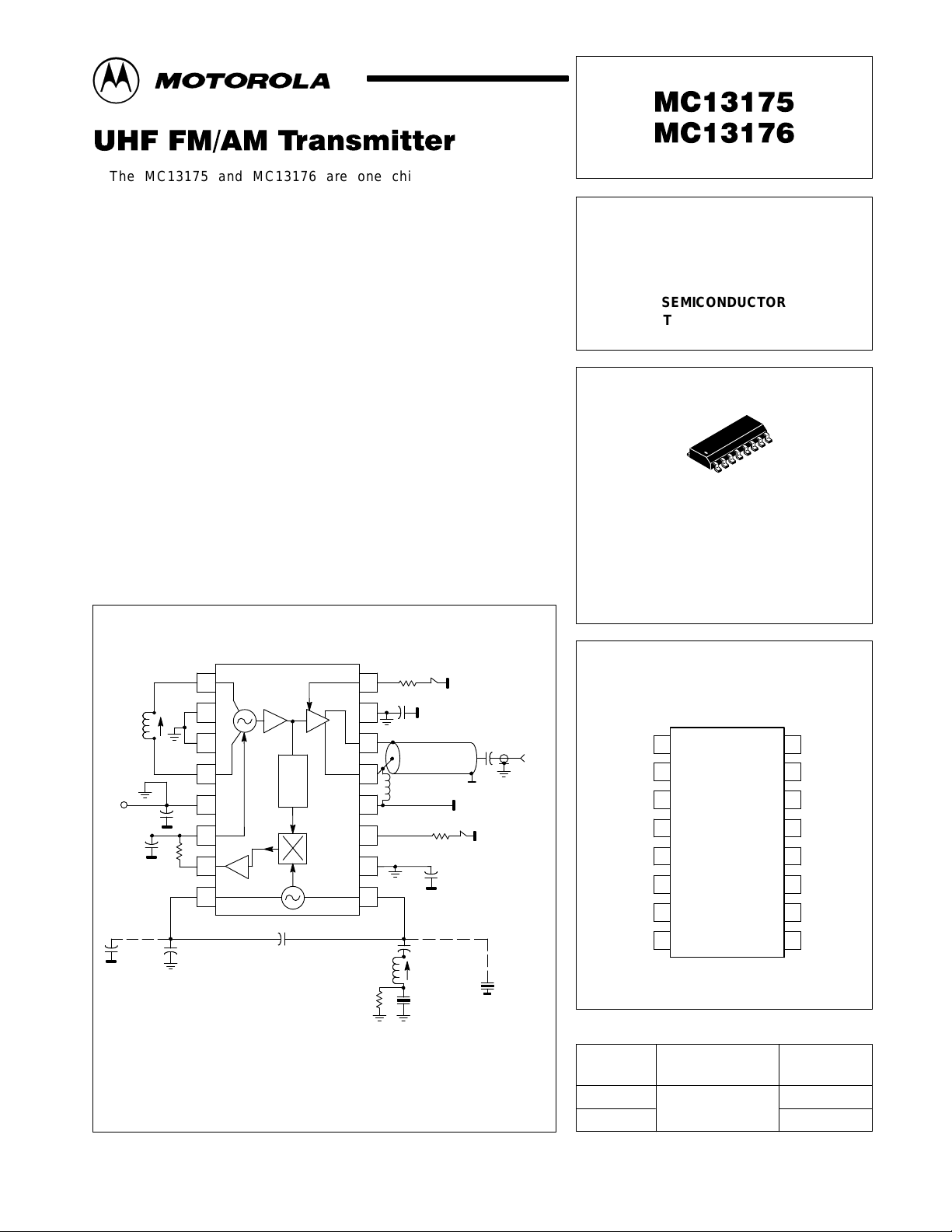
Figure 1. T ypical Application as 320 MHz AM Transmitter
AM Modulator
Tank
Coilcraft
150–05J08
(2)
V
EE
150p
Osc
0.1
µ
0.165
1.0k
1
2
3
µ
4
f/N
5
6
7
8
100p
(MC13176)
V
CC
1. 50 Ω coaxial balun, 1/10 wavelength at 320 MHz equals 1.5 inches.
NOTES:
2. Pins 5, 10 & 15 are ground and connected to VEE which is the component/DC ground plane
2. side of PCB. These pins must be decoupled to VCC; decoupling capacitors should be placed
2. as close as possible to the pins.
3. The crystal oscillator circuit may be adjusted for frequency with the variable inductor
3. (MC13175); recommended source is Coilcraft “slot seven” 7mm tuneable inductor, Part
3. #7M3–821. 1.0k resistor. Shunting the crystal prevents it from oscillating in the fundamental
3. mode.
30p
(MC13175)
MC13175–30p
MC13176–180p
3rd Overtone
40.0000 MHz
MC13175
Crystal
16
15
14
13
12
11
10
1.0k
9
0.82
1.3k
S
2
µ
0.01
V
EE
(1)
Z = 50
RFC
1
EE
27k
µ
0.01
MC13176
(3)
Fundamental
0.1
Crystal
10 MHz
V
µ
PIN CONNECTIONS
I
1
150p
Ω
V
CC
S
1
µ
V
CC
SMA
RF
out
Osc 1
NC
NC
Osc 4
V
EE
I
Cont
PD
out
Xtale
2
3
4
5
6
7
8
16
15
14
13
12
11
10
9
mod
Out
Gnd
Out 2
Out 1
V
CC
Enable
Reg.
Gnd
Xtalb
ORDERING INFORMATION
Operating
Device
MC13175D
MC13176D
Temperature Range
TA = – 40° to +85°C
Package
SO–16
SO–16
MOTOROLA RF/IF DEVICE DATA
Motorola, Inc. 1998 Rev 1.1
1
MC13175 MC13176
MAXIMUM RATINGS ( T
Rating Symbol Value Unit
Power Supply Voltage V
Operating Supply Voltage Range V
Junction Temperature T
Operating Ambient Temperature T
Storage Temperature
ELECTRICAL CHARACTERISTICS (Figure 2; V
Supply Current (Power down: I11 & I16 = 0) – I
Supply Current (Enable [Pin 11] to VCC thru 30 k, I16 = 0) – I
Total Supply Current (Transmit Mode)
(I
= 2.0 mA; fo = 320 MHz)
mod
Differential Output Power (fo = 320 MHz; V
= 500 mV
I
mod
I
mod
Hold–in Range (± ∆f
MC13175 (see Figure 7)
MC13176 (see Figure 8)
Phase Detector Output Error Current
MC13175
MC13176
Oscillator Enable Time (see Figure 27) 11 & 8 t
Amplitude Modulation Bandwidth (see Figure 29) 16 BW
Spurious Outputs (I
Spurious Outputs (I
Maximum Divider Input Frequency
Maximum Output Frequency
* For testing purposes, VCC is ground (see Figure 2).
; fo = N x f
p–p
= 2.0 mA (see Figures 7 and 8)
= 0 mA
mod
mod
= 25°C, unless otherwise noted.)
A
Characteristic
ref
x N)
ref
= 2.0 mA)
= 0 mA)
ref
)
CC
CC
J
A
T
stg
[Pin 9]
7.0 (max) Vdc
1.8 to 5.0 Vdc
+150 °C
– 40 to + 85 °C
– 65 to +150 °C
= – 3.0 Vdc, TA = 25°C, unless otherwise noted.)*
EE
Pin Symbol Min Typ Max Unit
– I
13 & 14 P
13 & 14 ± ∆f
7 l
13 & 14
13 & 14
–
13 & 14
EE1
EE2
EE3
out
error
enable
AM
P
son
P
soff
f
div
f
o
– 0.5 – – µA
–18 –14 – mA
–39 –34 – mA
dBm
2.0
–
H
3.5
4.0
20
22
– 4.0 – ms
– 25 – MHz
–
–
–
–
+ 4.7
–45
6.5
8.0
25
27
–50
–50
950
950
–
–
–
–
–
–
–
–
–
–
MHz
µA
dBc
MHz
Figure 2. 320 MHz Test Circuit
Osc
Tank
(1)
EE
Coilcraft
150–03J0
8
0.1
µ
27p
10p
(MC13175)
V
15p
(MC13176)
NOTES: 1. VCC is ground; while VEE is negative with respect to ground.
2.Pins 5, 10 and 15 are brought to the circuit side of the PCB via plated through holes.
They are connected together with a trace on the PCB and each Pin is decoupled to V
3.Recommended source is Coilcraft “slot seven” inductor, part number 7M3–821.
0.098
10k
1
2
3
µ
4
5
6
7
8
2.2k
2
f/N
MC13175–30p
MC13176–33p
MC13175
Crystal
3rd Overtone
40 MHz
16
15
14
13
12
11
10
9
0.82
1.0k
(ground).
CC
I
mod
10k
µ
0.1
V
CC
(1)
0.01
µ
(3)
51
51
I
reg. enable
30k
0.1
µ
µ
MC13176
Crystal
Fundamental
10 MHz
0.1
µ
0.01
0.01
RF
CC
RF
out 1
out 2
µ
µ
V
MOTOROLA RF/IF DEVICE DATA
Pin Symbol
MC13175 MC13176
PIN FUNCTION DESCRIPTIONS
Internal Equivalent
Circuit
Description/External
Circuit Requirements
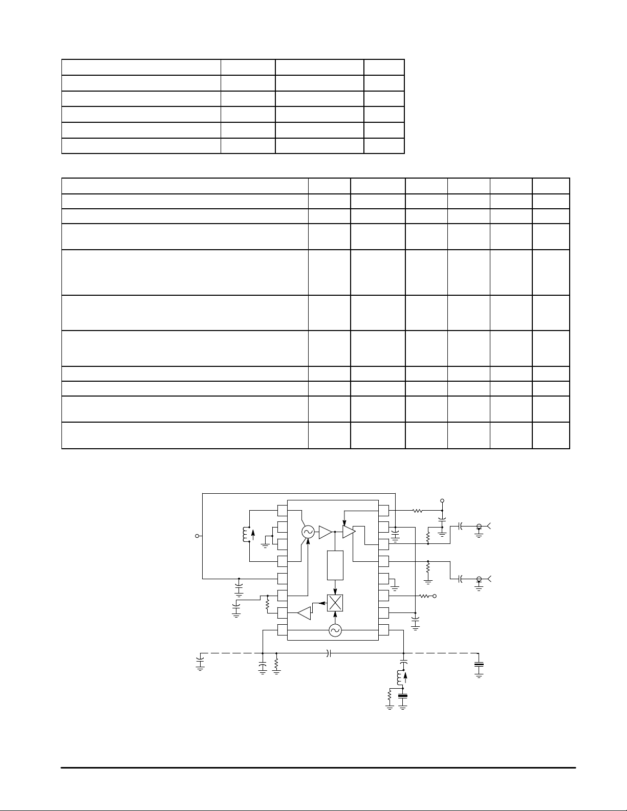
1 & 4 Osc 1,
Osc 4
5 V
6 I
EE
Cont
10k
1
0sc 1
V
EE
I
Cont
V
CC
10k
4
Osc 4
V
EE
5
6
Subcon
V
EE
V
CC
Reg
CCO Inputs
The oscillator is a current controlled type. An external oscillator
coil is connected to Pins 1 and 4 which forms a parallel
resonance LC tank circuit with the internal capacitance of the
IC and with parasitic capacitance of the PC board. Three
base–emitter capacitances in series configuration form the
capacitance for the parallel tank. These are the base–emitters
at Pins 1 and 4 and the base–emitter of the differential amplifier.
The equivalent series capacitance in the differential amplifier is
varied by the modulating current from the frequency control
circuit (see Pin 6, internal circuit). A more thorough discussion
is found in the Applications Information section.
Supply Ground (VEE)
In the PCB layout, the ground pins (also applies to Pins 10 and
15) should be connected directly to chassis ground. Decoupling
capacitors to VCC should be placed directly at
the ground returns.
Frequency Control
For VCC = 3.0 Vdc, the voltage at Pin 6 is approximately 1.55
Vdc. The oscillator is current controlled by the error current from
the phase detector. This current is amplified to drive the current
source in the oscillator section which controls the frequency of
the oscillator. Figures 9 and 10 show the ∆f
Figure 5 shows the ∆f
+85°C for 320 MHz. The CCO may be FM modulated as shown
in Figures 18 and 19, MC13176 320 MHz FM Transmitter. A
detailed discussion is found in the Applications Information
section.
osc
versus I
Cont
versus I
osc
at – 40°C, + 25°C and
Cont
,
7 PD
out
4.0k
MOTOROLA RF/IF DEVICE DATA
V
CC
4.0k
PD
out
7
Phase Detector Output
The phase detector provides ± 30 µA to keep the CCO locked at
the desired carrier frequency. The output impedance of the
phase detector is approximately 53 kΩ. Under closed loop
conditions there is a DC voltage which is dependent upon the
free running oscillator and the reference oscillator frequencies.
The circuitry between Pins 7 and 6 should be selected for
adequate loop filtering necessary to stabilize and filter the loop
response. Low pass filtering between Pin 7 and 6 is needed so
that the corner frequency is well below the sum of the divider
and the reference oscillator frequencies, but high enough to
allow for fast response to keep the loop locked. Refer to the
Applications Information section regarding loop filtering and FM
modulation.
3
MC13175 MC13176
9
ypp
5.0p
PIN FUNCTION DESCRIPTIONS
Pin Symbol
8 Xtale
9 Xtalb
10 Reg. Gnd
11 Enable
Internal Equivalent
Circuit
V
CC
Xtalb 12k8.0k
8
Xtale
V
CC
11
Enable
Subcon
10
Reg. Gnd
8.0k
5.0p
2.4k
4.0k
Reg
Description/External
Circuit Requirements
Crystal Oscillator Inputs
The internal reference oscillator is configured as a common
emitter Colpitts. It may be operated with either a fundamental
or overtone crystal depending on the carrier frequency and the
internal prescaler. Crystal oscillator circuits and specifications
of crystals are discussed in detail in the applications section.
With VCC = 3.0 Vdc, the voltage at Pin 8 is approximately 1.8
Vdc and at Pin 9 is approximately 2.3 Vdc. 500 to 1000 mVp–p
should be present at Pin 9. The Colpitts is biased at 200 µA;
additional drive may be acquired by increasing the bias to
approximately 500 µA. Use 6.2 k from Pin 8 to ground.
Regulator Ground
An additional ground pin is provided to enhance the stability of
the system. Decoupling to the VCC (RF ground) is essential; it
should be done at the ground return for Pin 10.
Device Enable
The potential at Pin 11 is approximately 1.25 Vdc. When Pin 11
is open, the transmitter is disabled in a power down mode and
draws less than 1.0 µA ICC if the MOD at Pin 16 is also open
(i.e., it has no current driving it). To enable the transmitter a
current source of 10 µA to 90 µA is provided. Figures 3 and 4
show the relationship between ICC, VCC and I
that ICC is flat at approximately 10 mA for I
100 µA (I
mod
= 0).
reg. enable
reg. enable
. Note
= 5.0 to
12 V
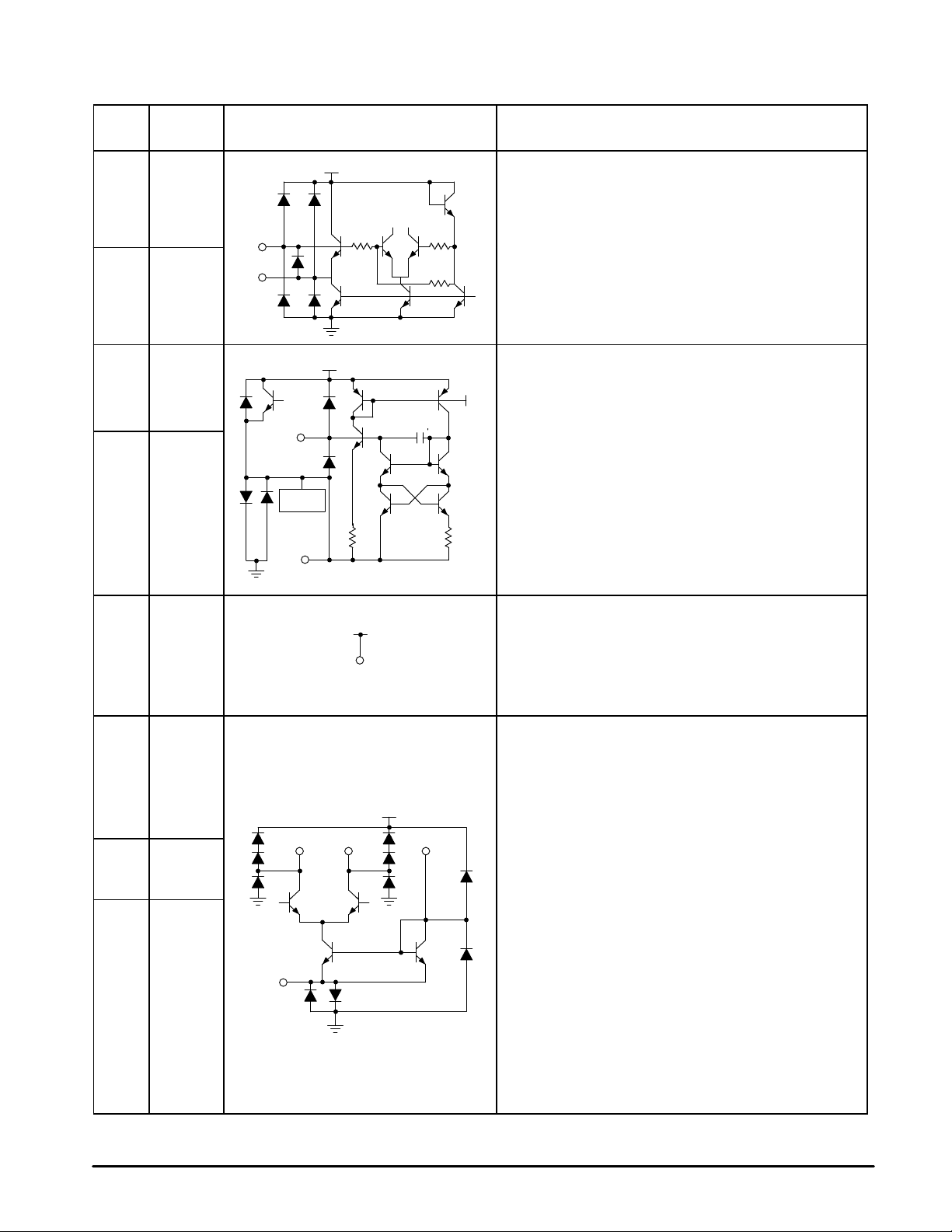
13 & 14 Out 1 and
15 Out_Gnd
16 I
CC
Out 2
mod
15
Out_Gnd
13
Supply Voltage (VCC)
V
CC
12
V
CC
V
CC
1614
I
Out 2Out 1
mod
The operating supply voltage range is from 1.8 Vdc to 5.0 Vdc.
In the PCB layout, the VCC trace must be kept as wide as
possible to minimize inductive reactances along the trace; it is
best to have it completely fill around the surface mount
components and traces on the circuit side of the PCB.
Differential Output
The output is configured differentially to easily drive a loop
antenna. By using a transformer or balun, as shown in the
application schematic, the device may then drive an unbalanced
low impedance load. Figure 6 shows how much the Output
Power and Free–Running Oscillator Frequency change with
temperature at 3.0 Vdc; I
Output Ground
This additional ground pin provides direct access for the output
ground to the circuit board VEE.
AM Modulation/Power Output Level
The DC voltage at this pin is 0.8 Vdc with the current source
active. An external resistor is chosen to provide a source
current of 1.0 to 3.0 mA, depending on the desired output power
level at a given VCC. Figure 28 shows the relationship of Power
Output to Modulation Current, I
power output can be acquired with about 35 mA ICC.
For FM modulation, Pin 16 is used to set the desired output
power level as described above.
For AM modulation, the modulation signal must ride on a
positive DC bias offset which sets a static (modulation off)
modulation current. External circuitry for various schemes is
further discussed in the Applications Information section.
mod
= 2.0 mA.
. At VCC = 3.0 Vdc, 3.5 dBm
mod
4
MOTOROLA RF/IF DEVICE DATA

MC13175 MC13176
DOCUMENT CONTAINS SCANNED IMAGES WHICH
COULD NOT BE PROCESSED FOR PDF FILES. FOR
COMPLETE DOCUMENT WITH IMAGES PLEASE
ORDER FROM MFAX OR THE LITERATURE
DISTRIBUTION CENTER
MOTOROLA RF/IF DEVICE DATA
5
MC13175 MC13176
10
8.0
6.0
4.0
, SUPPLY CURRENT (mA)
CC
2.0
I
0
10
5.0
0
– 5.0
, OSCILLAT OR FREQUENCY (MHz)
–10
OSC
f
∆
–15
–40
Figure 3. Supply Current
versus Supply V oltage
I
reg. enable
I
mod
0
1.0 2.0 3.0 4.0 5.0
VCC, SUPPLY VOLTAGE (Vdc)
Figure 5. Change Oscillator Frequency
versus Oscillator Control Current
VCC = 3.0 Vdc
I
= 2.0 mA
mod
f = 320 MHz (I
Free–Running Oscillator
– 20 0 20 40 80
I
, OSCILLAT OR CONTROL CURRENT (
Cont
Cont
= 90 µA
= 0
= 0; TA = 25
– 40 °C
25 °C
85
60
µ
A)
Figure 4. Supply Current versus
Regulator Enable Current
100
VCC = 3.0 Vdc
I
= 0
mod
10
, SUPPLY CURRENT (mA)
CC
I
1.0
0.1
1.0 10 100 1000
I
reg. enable
, REGULAT OR ENABLE CURRENT (µA)
Figure 6. Change in Oscillator Frequency and
Output Power versus Ambient Temperature
4.0
∆
f
osc
3.0
°
C)
°
C
2.0
1.0
–1.0
– 2.0
, OSCILLAT OR FREQUENCY (MHz)
– 3.0
OSC
f
∆
– 4.0
0
–50
VCC = 3.0 Vdc
I
= 2.0 mA
mod
f = 320 MHz (I
Free–Running Oscillator
0 50 100
TA, AMBIENT TEMPERATURE (
= 0; TA = 25
Cont
°
C)
°
C)
5.5
P
O
5.0
4.5
4.0
, OUTPUT POWER (dBm)
O
3.5
P
3.0
41.0
40.8
40.6
40.4
40.2
40.0
39.8
, REFERENCE OSCILLAT OR FREQUENCY (MHz)
39.6
ref
–30
f
6
Figure 7. MC13175 Reference Oscillator
Frequency versus Phase Detector Current
Closed Loop Response:
VCC = 3.0 Vdc
I
= 2.0 mA
mod
ICC = 36 mA
PO = 5.4 dBm
– 20 –10 10 20 300
I7, PHASE DETECTOR CURRENT (
fo = 8.0 x f
V
ref
= 500 mV
ref
I
mod
ICC = 25 mA
PO = – 0.2 dBm
µ
A)
p–p
= 1.0 mA
10.3
10.2
10.1
10
9.9
, REFERENCE OSCILLAT OR FREQUENCY (MHz)
9.8
–30
ref
f
Figure 8. MC13176 Reference Oscillator
Frequency versus Phase Detector Current
Closed Loop Response:
VCC = 3.0 Vdc
fo = 32 x f
ref
V
= 500 mV
I
= 2.0 mA
mod
ICC = 35.5 mA
PO = 4.7 dBm
– 20 –10 10 20 300
I7, PHASE DETECTOR CURRENT (
ref
p–p
I
= 1.0 mA
mod
ICC = 22 mA
PO = –1.1 dBm
µ
A)
MOTOROLA RF/IF DEVICE DATA
 Loading...