

Motorola MC13173FTB Datasheet
1
MOTOROLA ANALOG IC DEVICE DATA
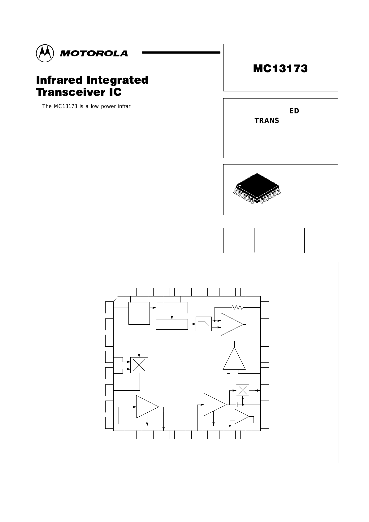
The MC13173 is a low power infrared integrated system (IRIS). It is a
unique blend of a split IF wideband FM receiver and a specialized infrared
LED transmitter. This device was designed to provide communications
between portable computers via a half duplex infrared link at data rates up to
200 kbps.
The receiver includes a mixer, IF amplifier and limiter and data slicer. The
IF amplifier is split to accommodate two low cost cascaded filters. The RSSI
output is derived by summing the output of both IF sections.
The transmitter section includes a frequency synthesizer, FSK modulator ,
harmonic low pass filter and an IR LED driver.
• Transmitter Operates in Two Modes:
– On/Off Pulsing for Remote Control
– FSK Modulation at 1.4 MHz for Data Communications
• Over 70 dB of RSSI Range
• Split IF for Improved Filtering and Extended RSSI Range
• Digitally controlled Via a Six Line Interface Bus
• Individual Circuit Blocks Can Be Powered Down When Not In Use for
Power Conservation
Device
Operating
Temperature Range
Package
SEMICONDUCTOR
TECHNICAL DATA
INFRARED
TRANSCEIVER
ORDERING INFORMATION
MC13173FTB TA = – 40° to +85°C TQFP–32
FTB SUFFIX
PLASTIC PACKAGE
CASE 873
(Thin QFP)
Order this document by MC13173/D
32
1
Simplified Block Diagram
This device contains 914 active transistors.
32 kHz Ma Tx 14 MHz
T
Data
E
IR LED
32 31 30 29 28 27 26 25
24
23
22
21
20
19
18
17
9 10111213141516
IF IF IF V Lim Lim Lim RSSI
1
2
3
4
5
6
7
8
Master
FSK
Mode Select
Harmonic
Driver
Data Slicer
V
Limiter
IF
Mixer
Dec1 Dec2 Out
CC2
In Dec1 Dec2
12 M
V
R
RF In1
RF In2
Mixer
V
IF In
LED Driver
V
Data Out
V
Data
Demod
Quad Coil
Carrier
Ref PLL PLL Ref In Driver
Feedback
EE3
EE2
Slicer In
Detect
VCO/PLL
Modulator
LPF
Amplifier
Reg1
V
Reg2
EE1
Out
CC1
Motorola, Inc. 1996 Rev 0
MC13173
2
MOTOROLA ANALOG IC DEVICE DATA
MAXIMUM RATINGS
Rating Symbol Value Unit
Power Supply Voltage VCC – V
EE
6.0 Vdc
Junction Temperature T
J
150 °C
Storage Temperature T
stg
– 55 to +150 °C
NOTE: Devices should not be operated at or outside these values. The “Recommended Operating
Conditions” table provides for actual device operation.
RECOMMENDED OPERATING CONDITIONS
Characteristic Symbol Value Unit
Power Supply Voltage VCC – V
EE
2.7 to 5.5 Vdc
Ambient Temperature Range T
A
– 40 to +85 °C
DC ELECTRICAL CHARACTERISTICS (T
A
= +25°C, VCC = 3.3 Vdc, f
REF
= 32.768 kHz. Measured using test circuit in Figure 1,
unless otherwise noted.)
Characteristic
Pin Symbol Min Typ Max Unit
Supply Current (See Table 2) Control Pin
Logic State
7, 12 I
CC
Receive Mode
Communications Mode
A/V Mode
Standby Mode
TR E
01 0
10 0
10 1
00 0
–
–
–
–
6.5
4.75
1.5
<10
9.0
8.0
–
–
mA
nA
Master PLL Charge Current 31 I
MA
– ±25 – µA
DATA SLICER
Data Slicer Threshold Voltage 20 V
TH1
0.85 1.1 1.4 Vdc
Maximum Pull–Down Current 22 I
DS
1.0 1.8 – mA
CARRIER DETECT
Carrier Detect Threshold Voltage 16 V
TH2
1.0 1.15 1.3 Vdc
Maximum Pull–Down Current 17 I
CD
1.1 3.0 – mA
TRANSMITTER
Maximum Pull–Up Current 25 I
OH
5.8 7.0 – mA
Maximum Pull–Down Current 25 I
OL
– 150 700 µA
DC Output Voltage 24 V
O
– 200 – mV
Transmit PLL Charge Current 30 I
TX
– ±25 – µA
AC ELECTRICAL CHARACTERISTICS (T
A
= +25°C, VCC = 3.3 Vdc, f
REF
= 32.768 kHz. Measured using test circuit in
Figure 1, unless otherwise noted.)
Characteristic
Pin Symbol Min Typ Max Unit
TRANSMITTER
Upper Sideband Frequency (Mark) 24 f
HI
– 1.427 – MHz
Lower Sideband Frequency (Space) 24 f
LO
– 1.317 – MHz
Upper and Lower Sideband Amplitude 24 V
SB
40 54 70 mVrms
RECEIVER
Receiver Sensitivity – 12 dB SINAD 4, 19 V
SIN
– 5.0 – µV
MIXER
Mixer Conversion Gain 4, 5, 6 AV
(Mix)
– 23.5 – dB
Mixer Output Impedance 6 Z
O
– 330 – Ω
MC13173
3
MOTOROLA ANALOG IC DEVICE DATA
AC ELECTRICAL CHARACTERISTICS (continued) (T
A
= +25°C, VCC = 3.3 Vdc, f
REF
= 32.768 kHz. Measured using test circuit in
Figure 1, unless otherwise noted.)
Characteristic UnitMaxTypMinSymbolPin
IF AMPLIFIER
IF Amplifier Gain 8, 11 – – 54 – dB
IF Amplifier RSSI Slope 16 – – 275 – nA/dB
Input Impedance 8 Z
IN
– 330 – Ω
Output Impedance 11 Z
O
– 330 – Ω
RSSI Current Range 16 – – 20 – µA
RSSI Dynamic Range 16 – – 70 – dB
LIMITING AMPLIFIER
Input Impedance 13 Z
IN
– 330 – Ω
Limiter RSSI Slope 16 – – 360 – nA/dB
RSSI Current Range 16 – – 20 – µA
RSSI Dynamic Range 16 – – 58 – dB
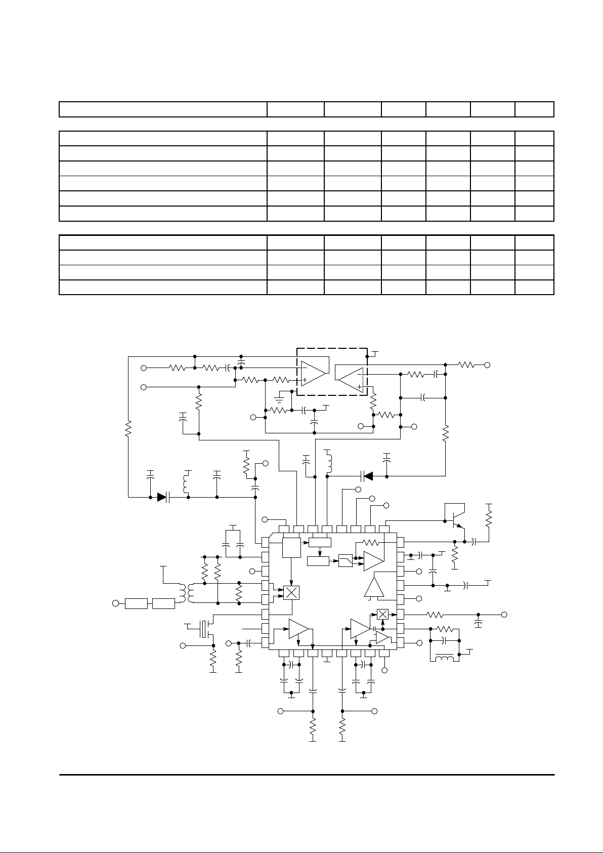
Figure 1. Test Circuit
10 k 127 k
100 k 100 k
10 k
– 1V
24.9 k
100 p
36 k
V
100 pF
MV209
MV209
10 k 10 k
200
ATTENLPF
F1
330 50
MC13173
50
10 p
100 nF
10 nF
100 k
100 k
20 p
100 p200 k
10 k
10 k
2N2222A 10 k
100
100 n
100 n
10 k
6.81 k
150 p
1.0 n
CC
V
CCVCC
V
CC
V
CC
0.1 F
µ
0.001 Fµ0.1 H
µ
V
CC
V
CC
– 1VV
CC
V
CC
0.001 F
µ
0.1 F
µ
V
EE
V
CC
V
CC
0.3 H
µ
100 p
V
CC
0.001 F
µ
0.1 H
µ
V
CC
V
CC
V
CC
V
CC
V
CC
V
CC
V
EE
V
CC
V
CC
V
CC
V
CC
V
EE
V
EE
0.1 F
µ
33 F
µ
V
EE
V
CC
0.1 F
µ
1.0 H
µ
100 n
V
CC
V
CC
1.0 n
100 n
0.1 F
µ
0.1 F
µ
ΩΩ
330
Ω
50
Ω
MC33202
32 25
916
17
24
8
1
V
CCVCC
+
V
CC
0.1 F
µ
1.0 n
1.0 n
V
CC
MC13173
4
MOTOROLA ANALOG IC DEVICE DATA
CIRCUIT DESCRIPTION
General
The MC13173 infrared transceiver integrates a split IF
wideband FM receiver and an IR LED transmitter into a single
IC. The transmitter is comprised of an FSK modulator,
harmonic low pass filter, and IR LED driver. The receiver
consists of a mixer, IF amplifier and limiting IF, detector, and
data slicer. It includes RSSI and carrier detect functions.
The transmitter is capable of two modes of operation. It
was primarily designed for use in the Communications Mode,
which enables point–to–point data links, such as the
communication from keyboard to computer, or for the
exchange of data between portable computers. In this mode
it is capable of 200 kbps half duplex FSK operation.
The transmitter can also operate in an “A/V” Mode, which
pulses the LED on and off with no carrier. (See Figure 11).
Digital Interface Bus
The MC13173 is controlled via a six line 3.3 V digital
interface bus. That includes three control pins, data in and
out pins, and a carrier detect pin. Listed below is a brief
description of each pin and its function.
Table 1. Digital Interface Pin Descriptions
Pin Pin Name Symbol I/O Description
28 Transmit Enable T I High – Transmitter is enabled
Low – Transmitter is disabled
27 Data In DI I Data Input – 38.2 kbps
Communication Mode
3 Receive Enable R I High – Receiver is enabled
Low – Receiver is disabled
22 Data Out DO O Demodulated Output Signal
17 Carrier Detect CD O High – Carrier is present
Low – Carrier is not present
26 Transmit Modulation Enable E I High – Transmitter is in A/V Mode
Low – Transmitter is in
Communications Mode
This transceiver was designed for use in battery powered,
hand–held consumer products. To minimize power
consumption, the digital interface enables individual system
blocks to be powered down while not in use. The following
diagram shows the mode of the IC and the power state of
each circuit block for a given set of control levels.
Table 2. Power State Table
Control
Pins*
Circuit Block Power States
(See Figures 2 and 3)
T R E
Mode
Master
VCO
FSK
Modulator
Receiver
LED
Driver
Supply
Current
(Typical)
0 0 0 OFF Off Of f Off Off 10 nA
0 0 1 OFF Off Of f Off Off 70 µA
0 1 X Receive On Off On Off 6.5 mA
1 1 1 Receive On Off On On 7.5 mA
1 1 0 Transmit – Comm Mode On On On On 9.0 mA
1 0 0 Transmit – Comm Mode On On Off On 4.75 mA
1 0 1 Transmit – A/V Mode Of f Off Of f On 1.5 mA
* With Data In Pin Low

MC13173
5
MOTOROLA ANALOG IC DEVICE DATA
Master VCO/PLL
The master VCO provides the reference frequency for the
FSK modulator and the LO frequency for the receiver
downconverter. With a 32.768 kHz input frequency to the
master VCO on Pin 1, the LO frequency for the receiver will
be at 12.075 MHz. The reference frequency for the FSK
modulator will be at approximately 1.1 MHz. The master VCO
and FSK modulator are not used when the transmitter is used
in A/V mode, and both are powered down.
Receiver Description
The single conversion receiver portion of the MC13173 is
low power and wideband, and incorporates a split IF. This
section includes a mixer, IF amplifier, limiting IF, quadrature
detector and data slicer.
Mixer
The mixer is a double balanced four quadrant multiplier. It
can be driven either differentially or single–ended by
connecting the unused input to the positive supply rail.
The buffered output is internally loaded for an output
impedance of 330 Ω for use with a standard ceramic filter.
IF Amplifier
The first IF amplifier section is composed of three
differential stages with the second and third stages
contributing to the RSSI. This section has internal DC
feedback and external input decoupling for improved
symmetry and stability. The total gain of the IF amplifier block
is approximately 40 dB. The fixed internal input impedance is
330 Ω for use with a 10.7 MHz ceramic filter . The output of the
IF amplifier is buffered and the impedance is 330 Ω .
Limiter
The limiter section is similar to the IF amplifier section,
except that four stages are used with the last three
contributing to the RSSI. This IF limiting amplifier section
drives the quadrature detector internally.
RSSI/Carrier Detect
The received signal strength indicator (RSSI) outputs a
current proportional to the log of the received signal
amplitude. The RSSI current output is derived by summing
the currents from the IF and limiting amplifier stages. An
external resistor sets the output voltage range.
The carrier detect threshold is set at approximately
1.2 Vdc. When the RSSI level exceeds that threshold, the
carrier detect output will go high. A large resistor may be
added externally between the comparator output and the
positive input for hysteresis.
Quadrature Detector
The demodulator is a conventional quadrature type with
an external LC tank driven through an internal 5 pF capacitor.
The output is buffered to give an output impedance of less
than 1.0 kΩ at an average DC level of around 1.1 V.
Data Slicer
The data slicer is designed to square up the data signal. It
is self centering at about 1.1 V , and clips at about 0.75 V and
1.45 V . There is a short time constant for large peak–to–peak
voltage swings or when there is a change in DC level at the
detector output. The time constant is longer for small signals
or for continuous bits of the same polarity which drift close to
the threshold voltage.
Transmission Description
The MC13173 uses a dual modulus PLL to frequency shift
key (FSK) modulate the baseband digital input signal,
producing the necessary logic high and low frequencies for
transmission. The transmit frequency for a logic high is
1.427 MHz, and the frequency for a low is 1.317 MHz with a
32.768 kHz reference frequency.
FSK Modulator
In the communications mode, the FSK modulator uses the
reference frequency from the Master VCO to produce the two
frequencies required for a logic high and a logic low. In the
A/V mode, the FSK modulator is not used and is powered
down.
LED Driver Stage
A low pass filter following the FSK modulator removes the
undesired harmonic frequencies from the square–wave
output of the divider circuits in PLLs. The resulting sinusoidal
waveforms are fed into a unity gain difference amplifier,
which drives the base of an external transistor, modulating
the IR LED.
In A/V mode, the data is input directly into the inverting
input of the op amp, and the low pass filter is not used.

MC13173
6
MOTOROLA ANALOG IC DEVICE DATA
DOCUMENT CONTAINS SCANNED IMAGES WHICH
COULD NOT BE PROCESSED FOR PDF FILES. FOR
COMPLETE DOCUMENT WITH IMAGES PLEASE
ORDER FROM MFAX OR THE LITERATURE
DISTRIBUTION CENTER
 Loading...