

Motorola MC13158FTB Datasheet
Order this document by MC13158/D
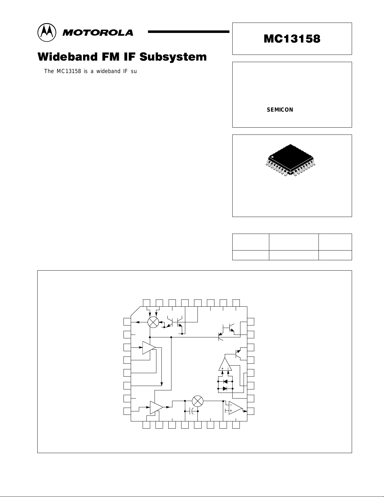
The MC13158 is a wideband IF subsystem that is designed for high
performance data and analog applications. Excellent high frequency
performance is achieved, with low cost, through the use of Motorola’s
MOSAIC 1.5 RF bipolar process. The MC13158 has an on–board
grounded collector VCO transistor that may be used with a fundamental or
overtone crystal in single channel operation or with a PLL in multi–channel
operation. The mixer is useful to 500 MHz and may be used in a balanced
differential or single ended configuration. The IF amplifier is split to
accommodate two low cost cascaded filters. RSSI output is derived by
summing the output of both IF sections. A precision data shaper has an Off
function to shut the output off to save current. An enable control is provided
to power down the IC for power management in battery operated
applications.
Applications include DECT , wideband wireless data links for personal and
portable laptop computers and other battery operated radio systems which
utilize GFSK, FSK or FM modulation.
• Designed for DECT Applications
• 1.8 to 6.0 Vdc Operating Voltage
• Low Power Consumption in Active and Standby Mode
• Greater than 600 kHz Detector Bandwidth
• Data Slicer with Special Off Function
• Enable Function for Power Down of Battery Operated Systems
• RSSI Dynamic Range of 80 dB Minimum
• Low External Component Count
WIDEBAND FM IF
SUBSYSTEM FOR DECT
AND DIGITAL APPLICATIONS
SEMICONDUCTOR
TECHNICAL DATA
32
1
FTB SUFFIX
PLASTIC PACKAGE
CASE 873
(Thin QFP)
ORDERING INFORMATION
Operating
Device
MC13158FTB TA = – 40 to +85°C TQFP–32
Temperature Range
Package
Mix Out
V
CC1
IF In
IF Dec1
IF Dec2
IF Out
V
CC2
Lim In
Representative Block Diagram
Osc
N/C
11
N/C
Osc
Emit
MC13158
Data
Slicer
5.0 p
12
Lim
Out
Base
13
Quad
Mix
Mix
In1
In2
1
2
3
4
5
6
7
8
IF Amp
LIM
Amp
10
9
Lim
Lim
Dec2
Dec1
This device contains 234 active transistors.
N/C
14
N/C
EE1
15
Det
Gain
EnableV
Bias
V
2532 31 30 29 28 27 26
16
EE2
24
23
22
21
20
19
18
17
RSSI
RSSI Buf
DS Gnd
DS Out
DS In2
DS “off”
DS In1
Det Out
MOTOROLA ANALOG IC DEVICE DATA
Motorola, Inc. 1996 Rev 1
1

MC13158
MAXIMUM RATINGS
Rating Pin Symbol Value Unit
Power Supply Voltage 16, 26 V
Junction Temperature T
Storage Temperature Range T
NOTE: 1.Devices should not be operated at or outside these values. The “Recommended Operating
Conditions” provide for actual device operation.
S(max)
JMAX
stg
6.5 Vdc
+150 °C
–65 to +150 °C
RECOMMENDED OPERATING CONDITIONS (V
Rating
Power Supply Voltage 2, 7 V
TA = 25°C
–40°C ≤ TA≤ 85°C 16, 26
Input Frequency 31, 32 F
Ambient Temperature Range T
Input Signal Level 31, 32 V
DC ELECTRICAL CHARACTERISTICS (T
Characteristic
Total Drain Current VS = 2.0 Vdc 16, 26 I
DATA SLICER (Input Voltage Referenced to VEE; VS = 3.0 Vdc; No Input Signal)
Output Current; V18 LO; V19 = V
Data Slicer Enabled (DS “on”) V18 < V
Output Current; V18 HI; V19 = V
Data Slicer Enabled (DS “on”) V18 > V
Output Current; V19 = V
Data Slicer Disabled (DS “off”) V20 = VS/2
= 25°C; VS = 3.0 Vdc; No Input Signal; See Figure 1.)
A
Condition Pin Symbol Min Typ Max Unit
VS = 3.0 Vdc 3.5 5.7 8.5
VS = 6.0 Vdc 3.5 6.0 9.5
See Figure 2
V20 = VS/2
See Figure 3
V20 = VS/2
See Figure 4
= V2 = V7; VEE = V16 = V22 = V26; VS = VCC – VEE)
CC
Pin Symbol Value Unit
TOTAL
EE
20
EE
20
CC
21 I
21 I
21 I
21
21
21
S
in
A
in
2.5 5.5 8.5 mA
2.0 5.9 – mA
– 0.1 1.0 µA
– 0.1 1.0 µA
2.0 to 6.0 Vdc
10 to 500 MHz
–40 to +85 °C
200 mVrms
AC ELECTRICAL CHARACTERISTICS (T
Characteristic
MIXER
Mixer Conversion Gain Vin = 1.0 mVrms 31, 32, 1 – – 22 – dB
Noise Figure Input Matched 31, 32, 1 NF – 14 – dB
Mixer Input Impedance Single–Ended 31, 32 Rp – 865 – Ω
Mixer Output Impedance 1 – – 330 – Ω
2
= 25°C; VS = 3.0 Vdc; fRF = 110.7 MHz; fLO = 100 MHz; See Figure 1.)
A
Condition Pin Symbol Min Typ Max Unit
See Figure 5
See Figure 15 Cp – 1.6 – pF
MOTOROLA ANALOG IC DEVICE DATA
MC13158
AC ELECTRICAL CHARACTERISTICS (continued) (T
Characteristic
IF AMPLIFIER SECTION
IF RSSI Slope See Figure 8 23 – 0.15 0.3 0.4 µA/dB
IF Gain f = 10.7 MHz 3, 6 – – 36 – dB
Input Impedance 3 – – 330 – Ω
Output Impedance 6 – – 330 – Ω
LIMITING AMPLIFIER SECTION
Limiter RSSI Slope See Figure 9 23 – 0.15 0.3 0.4 µA/dB
Limiter Gain f = 10.7 MHz 8, 12 – – 70 – dB
Input Impedance 8 – – 330 – Ω
Condition Pin Symbol Min Typ Max Unit
See Figure 7
= 25°C; VS = 3.0 Vdc; fRF = 110.7 MHz; fLO = 100 MHz; See Figure 1.)
A
Figure 1. T est Circuit
Osc
Emit
MC13158
Lim
Out
12
LO Input
5.0 p
Base
13
100 MHz
200 mVrms
N/COsc
Data
Slicer
N/CQuad
14
100 k
1.0
µ
H
–3.0 Vdc
50
A
Det
Gain
15
V
EE1
Bias
2532 31 30 29 28 27 26
Enable
RSSI
RSSI
Buf
DS
Gnd
DS
Out
DS
In2
DS
“off”
DS
In1
Det
Out
V
EE2
16
A
51 k
24
23
22
21
20
19
18
17
–2.3 Vdc
A
0 to –3.0 Vdc
100
µ
A
A
–1.5 Vdc
0 to –3.0 Vdc
V
–3.0 Vdc
–3.0 Vdc
Mixer
Output
IF
Input
IF
Output
Limiter
Input
110.7 MHz
330
50
330
50
RF Input
1.0 n
100 n
1.0 n
100 n
1.0 n
100 n
100 n
1
2
3
4
5
6
7
8
1:4
Mix
Out
V
CC1
IF
In
IF
Dec1
IF
Dec2
IF
Out
V
CC2
Lim
In
Mix
In2
Lim
Dec1
9
200
Lim
Dec2
100 n
In1
Lim Amp
N/C
10
1.0 n1.0 n
N/CMix
11
MOTOROLA ANALOG IC DEVICE DATA
200 pF
6.8 k
–3.0 Vdc
3
MC13158
T ypical Performance Over Temperature
(per Figure 1)
6.4
6.2
6.0
5.8
5.6
5.4
5.2
, TOTAL SUPPLY CURRENT (mA)
5.0
TOTAL
I
4.8
0.12
Data Slicer “On”
µ
V19 = V
0.10
V20 = VS/2
0.08
0.06
0.04
DATA SLICER OUTPUT CURRENT ( A)
0.02
–40
Figure 2. T otal Supply Current versus
Ambient T emperature, Supply Voltage
VS = 6.0 V
3.0 V
2.0 V
DATA SLICER OUTPUT CURRENT (mA)
–20
0 20 40 60 80 100 120 0 20 40 60 80 100 120
TA, AMBIENT TEMPERATURE (°C)
Figure 4. Data Slicer On Output Current
versus Ambient T emperature
V18 > V
20
CC
– 0.1
– 0.2
– 0.3
– 0.4
NORMALIZED MIXER GAIN (dB)
– 0.5
– 20 0 20 40 60 80 100 120 – 20 0 20 40 60 80 100 120
TA, AMBIENT TEMPERATURE (°C)
– 0.6
Figure 3. Data Slicer On Output Current
versus Ambient T emperature
8.5
Data Slicer “On”
V19 = V
8.0
7.5
7.0
6.5
6.0
5.5
5.0
EE
V20 = VS/2
–20
TA, AMBIENT TEMPERATURE (°C)
Figure 5. Normalized Mixer Gain
versus Ambient T emperature
0.2
0.1
0
–40
TA, AMBIENT TEMPERATURE (°C)
V18 < V
20
Vin = 1.0 mVrms
VS = 3.0 Vdc
fc = 110.7 MHz
fLO = 100 MHz
Figure 6. Mixer RSSI Output Current versus
Ambient T emperature, Mixer Input Level
7.0
µ
6.0
5.0
VS = 3.0 Vdc
fc = 110.7 MHz
fLO = 100 MHz
4.0
3.0
MIXER RSSI OUTPUT CURRENT ( A)
2.0
– 20 0 20 40 60 80 – 20 0 20 40 60 80 100 120100 120
–40
TA, AMBIENT TEMPERATURE (°C)
4
Vin = 10 mVrms
Vin = 1.0 mVrms
0.6
VS = 3.0 Vdc
0.4
f = 10.7 MHz
Vin = 1.0 mVrms
0.2
0
– 0.2
– 0.4
NORMALIZED IF AMP GAIN (dB)
– 0.6
– 0.8
–40
Figure 7. Normalized IF Amp Gain
versus Ambient T emperature
TA, AMBIENT TEMPERATURE (°C)
MOTOROLA ANALOG IC DEVICE DATA

MC13158
tT ypical Performance Over Temperature
(per Figure 1)
Figure 8. IF Amp RSSI Output Current versus
Ambient T emperature, IF Input Level
10
µ
9.0
8.0
7.0
VS = 3.0 Vdc
6.0
f = 10.7 MHz
5.0
4.0
3.0
IF AMP RSSI OUTPUT CURRENT ( A)
2.0
– 20 0 20 40 60 80 – 20 0 20 40 60 80 100 120100 120
–40
TA, AMBIENT TEMPERATURE (°C)
Figure 10. Total RSSI Output Current versus
Ambient T emperature (No Signal)
0.60
VS = 3.0 Vdc
µ
No Input Signal
0.55
0.50
0.45
Vin = 10 mVrms
Vin = 1.0 mVrms
Figure 9. Limiter Amp RSSI Output Current
versus Ambient T emperature, Input Signal Level
8.0
µ
Vin = 100 mVrms
6.0
LIMITER AMP RSSI OUTPUT CURRENT ( A)
4.0
2.0
– 2.0
VS = 3.0 Vdc
f = 10.7 MHz
0
–40
TA, AMBIENT TEMPERATURE (°C)
Vin = 10 mVrms
Vin = 1.0 mVrms
Vin = 100
Figure 11. Demodulator DC Voltage versus
Ambient Temperature
1.20
1.15
1.10
1.05
1.00
µ
Vrms
VS = 3.0 Vdc
R17 = 51 k
R15 = 100 k
0.40
TOTAL RSSI OUTPUT CURRENT ( A)
0.35
SYSTEM LEVEL AC ELECTRICAL CHARACTERISTICS (T
12 dB SINAD Sensitivity: fRF = 112 MHz 1 – dBm
Narrowband Application f
Without Preamp Figure 25 –101
With Preamp Figure 26 –113
Third Order Intercept Point f
1.0 dB Comp. Point VS = 3.5 Vdc 1.0 dB C.Pt. –39
NOTES: 1. Test Circuit & Test Set per Figure 24.
– 20 0 20 40 60 80 100 120
–40
TA, AMBIENT TEMPERATURE (°C)
Characteristic
f
f
RF2
2.Test Circuit & Test Set per Figure 27.
A
Condition Notes Symbol Typ Unit
= 1.0 kHz
mod
= ±125 kHz
dev
SINAD Curve
= 112 MHz 2 IIP3 –32 dBm
RF1
= 112.1 MHz
Figure 28
0.95
DEMODULATOR OUTPUT DC VOLTAGE (Vdc)
0.90
–40
– 20 0 20 40 60 80 100 120
TA, AMBIENT TEMPERATURE (°C)
= 25°C; VS = 3.0 Vdc; fRF = 112 MHz; fLO = 122.7 MHz)
MOTOROLA ANALOG IC DEVICE DATA
5

MC13158
CIRCUIT DESCRIPTION
General
The MC13158 is a low power single conversion wideband
FM receiver incorporating a split IF . This device is designated
for use as the backend in digital FM systems such as Digital
European Cordless Telephone (DECT) and wideband data
links with data rates up to 2.0 Mbps. It contains a mixer,
oscillator, Received Signal Strength Indicator (RSSI), IF
amplifier, limiting IF, quadrature detector, power down or
enable function, and a data slicer with output off function.
Further details are covered in the Pin Function Description
which shows the equivalent internal circuit and external
circuit requirements.
Current Regulation/Enable
Temperature compensating voltage independent current
regulators which are controlled by the enable pin (Pin 25)
where “low” powers up and “high” powers down the entire
circuit.
Mixer
The mixer is a double–balanced four quadrant multiplier
and is designed to work up to 500 MHz. It can be used in
differential or in single ended mode by connecting the other
input to the positive supply rail. The linear gain of the mixer is
approximately 22 dB at 100 mVrms LO drive level. The mixer
gain and noise figure have been emphasized at the expense
of intermodulation performance. RSSI measurements are
added in the mixer to extend the range to higher signal levels.
The single–ended parallel equivalent input impedance of the
mixer is Rp ~ 1.0 kΩ and Cp ~ 2.0 pF. The buffered output of
the mixer is internally loaded resulting in an output
impedance of 330 Ω.
Local Oscillator
The on–chip transistor operates with crystal and LC
resonant elements up to 220 MHz. Series resonant, overtone
crystals are used to achieve excellent local oscillator stability .
Third overtone crystals are used through about 65 to 70 MHz.
Operation from 70 MHz up to 180 MHz is feasible using the
on–chip transistor with a 5th or 7th overtone crystal. To
enhance operation using an overtone crystal, the internal
transistor bias is increased by adding an external resistor
from Pin 29 to VEE; however, with an external resistor the
oscillator stays on during power down. Typically, –10 dBm of
local oscillator drive is needed to adequately drive the mixer.
With an external oscillator source, the IC can be operated up
to 500 MHz.
RSSI
The received signal strength indicator (RSSI) output is a
current proportional to the log of the received signal
amplitude. The RSSI current output is derived by summing
the currents from the mixer, IF and limiting amplifier stages.
An increase in RSSI dynamic range, particularly at higher
input signal levels is achieved. The RSSI circuit is designed
to provide typically 85 dB of dynamic range with temperature
compensation.
Linearity of the RSSI is optimized by using external
ceramic bandpass filters which have an insertion loss of
4.0 dB and 330 Ω source and load impedance. For higher
data rates used in DECT and related applications, LC
bandpass filtering is necessary to acquire the desired
bandpass response; however, the RSSI linearity will require
the same insertion loss.
RSSI Buffer
The RSSI output current creates a voltage across an
external resistor. A unity voltage–gain amplifier is used to
buffer this voltage. The output of this buffer has an active
pull–up but no pull–down, so it can also be used as a peak
detector. The negative slew rate is determined by external
capacitance and resistance to the negative supply .
IF Amplifier
The first IF amplifier section is composed of three
differential stages with the second and third stages
contributing to the RSSI. This section has internal DC
feedback and external input decoupling for improved
symmetry and stability. The total gain of the IF amplifier block
is approximately 40 dB at 10.7 MHz.
The fixed internal input impedance is 330 Ω. When using
ceramic filters requiring source and loss impedances of
330 Ω, no external matching is necessary. Overall RSSI
linearity is dependent on having total midband attenuation of
10 dB (4.0 dB insertion loss plus 6.0 dB impedance matching
loss) for the filter. The output of the IF amplifier is buffered
and the impedance is 330 Ω.
Limiter
The limiter section is similar to the IF amplifier section
except that five differential stages are used. The fixed internal
input impedance is 330 Ω. The total gain of the limiting
amplifier section is approximately 70 dB. This IF limiting
amplifier section internally drives the quadrature detector
section and it is also brought out on Pin 12.
Quadrature Detector
The quadrature detector is a doubly balanced four
quadrant multiplier with an internal 5.0 pF quadrature
capacitor between Pins 12 and 13. An external capacitor may
be added between these pins to increase the IF signal to the
external parallel RLC resonant circuit that provides the
90 degree phase shift and drives the quadrature detector. A
single pin (Pin 13) provides for the external LC parallel
resonant network and the internal connection to the
quadrature detector.
Internal low pass filter capacitors have been selected to
control the bandwidth of the detector. The recovered signal is
brought out by the inverting amplifier buffer. An external
feedback resistor from the output (Pin 17) to the input of the
inverting amplifier (Pin 15) controls the output amplitude; it is
combined with another external resistor from the input to the
negative supply (Pin 16) to set the output dc level. For a
resistor ratio of 1, the DC level at the detector output is
2.0 VBE (see Figure 12). A small capacitor C17 across the
first resistor (from Pin 17 to 15) can be used to reduce the
bandwidth.
Data Slicer
The data slicer is a comparator that is designed to square
up the data signal. Across the data slicer inputs (Pins 18
and 20) are back to back diodes.
6
MOTOROLA ANALOG IC DEVICE DATA

MC13158
Á
Á
Á
Á
Á
Á
Á
Á
Á
Á
Á
Á
Á
Á
Á
Á
Á
Á
Á
Á
Á
Á
Out
Á
Á
Á
Á
Á
Oscillator, and IF Amplifer. The operating
Á
Á
Á
Á
Á
Á
Á
Á
Á
Á
Á
Á
Á
Á
Á
Á
Á
Á
Á
Á
Á
Á
Á
Á
Á
Á
Á
Á
Á
Á
Á
Á
Á
Á
Á
Á
Á
Á
Á
Á
Á
Á
Á
Á
Á
Á
Á
Á
The recovered data signal from the quadrature detector
can be DC coupled to the data slicer DS IN1 (Pin 18). In the
application circuit shown in Figure 1 it will be centered at
2.0 VBE and allowed to swing ± VBE. A capacitor is placed
from DS IN2 (Pin 20) to VEE. The size of this capacitor and
the nature of the data signal determine how faithfully the data
slicer shapes up the recovered signal. The time constant is
short for large peak to peak voltage swings or when there is
a change in DC level at the detector output. For small signal
or for continuous bits of the same polarity which drift close to
the threshold voltage, the time constant is longer.
PIN FUNCTION DESCRIPTION
Pin
1
ÁÁ
ÁÁ
ÁÁ
2
ÁÁ
ÁÁ
ÁÁ
ÁÁ
ÁÁ
ÁÁ
3
ÁÁ
ÁÁ
ÁÁ
ÁÁ
4
Symbol
Mix
Out
ÁÁÁ
ÁÁÁ
ÁÁÁ
V
CC1
ÁÁÁ
ÁÁÁ
ÁÁÁ
ÁÁÁ
ÁÁÁ
ÁÁÁ
IF
In
ÁÁÁ
ÁÁÁ
ÁÁÁ
ÁÁÁ
IF
Internal Equivalent Circuit
26
2
V
V
CC1
EE1
БББББББББББББ
БББББББББББББ
БББББББББББББ
БББББББББББББ
БББББББББББББ
БББББББББББББ
БББББББББББББ
БББББББББББББ
БББББББББББББ
2
V
БББББББББББББ
CC1
БББББББББББББ
5
БББББББББББББ
IF Dec2
БББББББББББББ
330
Dec1
ÁÁ
5
ÁÁ
ÁÁ
ÁÁ
ÁÁÁ
IF
ÁÁÁ
Dec2
ÁÁÁ
ÁÁÁ
БББББББББББББ
БББББББББББББ
26
БББББББББББББ
V
EE1
БББББББББББББ
IF In
3
IF Dec1
A unique feature of the data slicer is that the inverting
switching stages in the comparator are supplied through the
emitter pin of the output transistor (Pin 22 – DS Gnd) to V
rather than internally to VEE. This is provided in order to
reduce switching feedback to the front end. A control pin is
provided to shut the data slicer output off (DS “off” – Pin 19).
With DS “off” pin at VCC the data slicer output is shut off by
shutting down the base drive to the output transistor. When a
channel is being monitored to make an RSSI measurement,
but not to collect data, the data output may be shut off to save
current.
Description/External Circuit Requirements
Mixer Output
The mixer output impedance is 330 Ω; it
ББББББББББББ
matches to 10.7 MHz ceramic filters with
330 Ω input impedance.
ББББББББББББ
ББББББББББББ
Mix
1
Supply V oltage (V
ББББББББББББ
This pin is the VCC pin for the Mixer, Local
supply voltage range is from 1.8 Vdc to
ББББББББББББ
5.0 Vdc. In the PCB layout, the VCC trace
ББББББББББББ
must be kept as wide as possible to minimize
inductive reactances along the trace; it is best
ББББББББББББ
to have it completely fill around the surface
ББББББББББББ
mount components and traces on the circuit
side of the PCB.
ББББББББББББ
CC1
)
IF Input
The input impedance at Pin 3 is 330 Ω. It
ББББББББББББ
64 k
64 k
matches the 330 Ω load impedance of a
ББББББББББББ
10.7 MHz ceramic filter. Thus, no external
matching is required.
ББББББББББББ
ББББББББББББ
IF DEC1 & DEC2
IF decoupling pins. Decoupling capacitors
should be placed directly at the pins to enhance
ББББББББББББ
stability . Two capacitors are decoupled to the
ББББББББББББ
RF ground V
ББББББББББББ
4
& DEC2.
ББББББББББББ
; one is placed between DEC1
CC1
EE
6
ÁÁ
ÁÁ
ÁÁ
ÁÁ
ÁÁ
ÁÁ
ÁÁ
ÁÁ
MOTOROLA ANALOG IC DEVICE DATA
IF
ÁÁÁ
Out
ÁÁÁ
ÁÁÁ
ÁÁÁ
ÁÁÁ
ÁÁÁ
ÁÁÁ
ÁÁÁ
БББББББББББББ
БББББББББББББ
БББББББББББББ
БББББББББББББ
БББББББББББББ
БББББББББББББ
БББББББББББББ
БББББББББББББ
2
V
CC1
26
V
EE1
IF
Out
IF Output
ББББББББББББ
The output impedance is 330 Ω; it matches
ББББББББББББ
the 330 input resistance of a 10.7 MHz
ceramic filter.
ББББББББББББ
5
ББББББББББББ
ББББББББББББ
ББББББББББББ
ББББББББББББ
ББББББББББББ
7

Pin
Á
Á
Á
Á
Á
Á
Á
Á
Á
Á
Á
Á
Á
Á
Á
Á
Á
Á
Á
Á
Á
Á
Á
Á
Limiter Decoupling
Á
Á
Á
Á
Á
Á
Á
Á
Á
Á
Á
Á
Á
Á
Á
Á
Á
Á
Á
Á
Á
Á
Á
Á
Á
Á
Á
Á
Á
Á
Á
Á
Á
Á
Á
Á
Á
Á
Á
Á
Á
Á
Á
Á
Á
Á
Á
Á
Á
Á
Á
Á
Á
Á
Á
Á
Á
Á
Á
Out
Á
Á
Á
Á
7
ÁÁ
ÁÁ
ÁÁ
8
ÁÁ
ÁÁ
9
ÁÁ
ÁÁ
10
ÁÁ
ÁÁ
1 1,14,
27 & 28
ÁÁ
ÁÁ
12
ÁÁ
ÁÁ
13
ÁÁ
ÁÁ
ÁÁ
ÁÁ
ÁÁ
ÁÁ
ÁÁ
15
ÁÁ
ÁÁ
17
ÁÁ
ÁÁ
ÁÁ
ÁÁ
ÁÁ
16
ÁÁ
ÁÁ
ÁÁ
ÁÁ
Symbol
V
CC2
ÁÁÁ
ÁÁÁ
ÁÁÁ
Lim
ÁÁÁ
In
ÁÁÁ
Lim
ÁÁÁ
Dec1
ÁÁÁ
Lim
ÁÁÁ
Dec2
ÁÁÁ
N/C
ÁÁÁ
ÁÁÁ
Lim
Out
ÁÁÁ
ÁÁÁ
Quad
ÁÁÁ
ÁÁÁ
ÁÁÁ
ÁÁÁ
ÁÁÁ
ÁÁÁ
ÁÁÁ
Det
ÁÁÁ
Gain
ÁÁÁ
Det
ÁÁÁ
Out
ÁÁÁ
ÁÁÁ
ÁÁÁ
ÁÁÁ
V
EE2
ÁÁÁ
ÁÁÁ
ÁÁÁ
ÁÁÁ
MC13158
PIN FUNCTION DESCRIPTION (continued)
Internal Equivalent Circuit
БББББББББББББ
7
V
16
7
V
V
CC2
EE2
10
Dec2
16
V
CC2
Lim
EE2
V
15
16
7
CC2
Det
Gain
V
EE2
330 64 k
Lim In
8
Lim Dec1
Lim
Quad
Out
12
13
5.0 p
64 k
9
17
Det
БББББББББББББ
БББББББББББББ
БББББББББББББ
БББББББББББББ
БББББББББББББ
БББББББББББББ
БББББББББББББ
БББББББББББББ
БББББББББББББ
БББББББББББББ
БББББББББББББ
БББББББББББББ
БББББББББББББ
БББББББББББББ
БББББББББББББ
БББББББББББББ
БББББББББББББ
БББББББББББББ
БББББББББББББ
БББББББББББББ
БББББББББББББ
БББББББББББББ
БББББББББББББ
БББББББББББББ
БББББББББББББ
БББББББББББББ
БББББББББББББ
БББББББББББББ
БББББББББББББ
БББББББББББББ
Description/External Circuit Requirements
Supply Voltage (V
ББББББББББББ
This pin is VCC supply for the Limiter,
Quadrature Detector, data slicer and RSSI
ББББББББББББ
buffer circuits. In the application PC board this
ББББББББББББ
pin is tied to a common VCC trace with V
Limiter Input
ББББББББББББ
The limiter input impedance is 330 Ω.
ББББББББББББ
Limiter Decou
ББББББББББББ
Decoupling capacitors are placed directly at
ББББББББББББ
these pins and to VCC (RF ground). Use the
ББББББББББББ
same procedure as in the IF decoupling.
ББББББББББББ
lin
CC2
)
CC1
No Connects
There is no internal connection to these pins;
ББББББББББББ
however it is recommended that these pins be
ББББББББББББ
connected externally to VCC (RF ground).
Limiter Output
The output impedance is low. The limiter
ББББББББББББ
drives a quadrature detector circuit with in–
ББББББББББББ
phase and quadrature phase signals.
Quadrature Detector Circuit
ББББББББББББ
The quadrature detector is a doubly balanced
ББББББББББББ
four–quadrant multiplier with an internal 5.0 pF
capacitor between Pins 12 and 13. An external
ББББББББББББ
capacitor may be added to increase the IF
ББББББББББББ
signal to Pin 13. The quadrature detector pin is
provided to connect the external RLC parallel
ББББББББББББ
resonant network which provides the 90 degree
ББББББББББББ
phase shift and drives the quadrature detector.
ББББББББББББ
Detector Buffer Amplifier
ББББББББББББ
This is an inverting amplifier. An external feed-
ББББББББББББ
back resistor from Pin 17 to 15, (the inverting
input) controls the output amplitude; another
ББББББББББББ
resistor from Pin 15 to the negative supply
ББББББББББББ
(Pin 16) sets the DC output level. A 1:1 resistor
ББББББББББББ
ratio sets the output DC level at two VBE with
respect to VEE. A small capacitor from Pin 17 to
ББББББББББББ
15 can be used to set the bandwidth.
ББББББББББББ
Supply Ground (V
ББББББББББББ
In the PCB layout, the ground pins (also applies
ББББББББББББ
to Pin 26) should be connected directly to
ББББББББББББ
chassis ground. Decoupling capacitors to V
should be placed directly at the ground pins.
ББББББББББББ
EE2
)
CC
.
8
MOTOROLA ANALOG IC DEVICE DATA
 Loading...