

Motorola MC13156DW, MC13156FB Datasheet
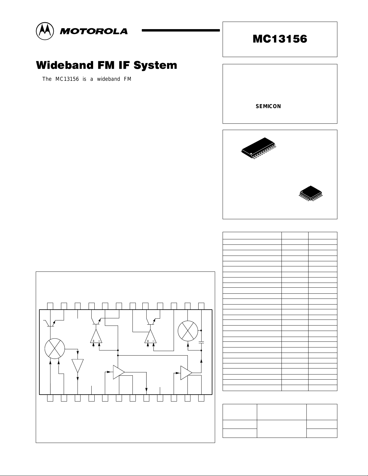
The MC13156 is a wideband FM IF subsystem targeted at high
performance data and analog applications. Excellent high frequency
performance is achieved at low cost using Motorola’s MOSAIC 1.5 bipolar
process. The MC13156 has an onboard grounded collector VCO transistor
that may be used with a fundamental or overtone crystal in single channel
operation or with a PLL in multichannel operation. The mixer is useful to
500 MHz and may be used in a balanced–differential, or single–ended
configuration. The IF amplifier is split to accommodate two low cost
cascaded filters. RSSI output is derived by summing the output of both IF
sections. A precision data shaper has a hold function to preset the shaper for
fast recovery of new data.
Applications for the MC13156 include CT–2, wideband data links and
other radio systems utilizing GMSK, FSK or FM modulation.
• 2.0 to 6.0 Vdc Operation
• Typical Sensitivity at 200 MHz of 2.0 µV for 12 dB SINAD
• RSSI Dynamic Range Typically 80 dB
• High Performance Data Shaper for Enhanced CT–2 Operation
• Internal 330 Ω and 1.4 kΩ Terminations for 10.7 MHz and 455 kHz Filters
• Split IF for Improved Filtering and Extended RSSI Range
• 3rd Order Intercept (Input) of –25 dBm (Input Matched)
Order this document by MC13156/D
WIDEBAND FM IF
SYSTEM FOR DIGITAL AND
ANALOG APPLICATIONS
SEMICONDUCTOR
TECHNICAL DATA
DW SUFFIX
24
1
FB SUFFIX
PLASTIC QFP PACKAGE
CASE 873
PLASTIC PACKAGE
CASE 751E
(SO–24L)
32
1
Simplified Block Diagram
DS
DS
Data
V
EE1
Mix
Out
CAR
Det
V
CC1
Bias
RSSI
IF
In
LO
LO
Emit
In
Mixer
RF
RF
In 2
In 1
NOTE: Pin Numbers shown for SOIC package only. Refer to Pin Assignments Table.
This device contains 197 active transistors.
V
EE2
IF
DEC 1
DS
Hold
IF Amp
DEC 2
18192022 1314151617212324
IF
Data
Slicer
Out
Out
Bias
IF
Gnd
V
CC2
In
LIM Amp
LIM
In
Demod
11
LIM
DEC 1
Quad
Coil
1210987654321
LIM
DEC 2
5.0
pF
PIN CONNECTIONS
Function
RF Input 1
RF Input 2
Mixer Output
V
CC1
IF Amp Input
IF Amp Decoupling 1
IF Amp Decoupling 2
VCC Connect (N/C Internal)
IF Amp Output
V
CC2
Limiter IF Input
Limiter Decoupling 1
Limiter Decoupling 2
VCC Connect (N/C Internal)
Quad Coil
Demodulator Output
Data Slicer Input
VCC Connect (N/C Internal)
Data Slicer Ground
Data Slicer Output
Data Slicer Hold
V
EE2
RSSI Output/Carrier Detect In
Carrier Detect Output
V
and Substrate
EE1
LO Emitter
LO Base
VCC Connect (N/C Internal)
ORDERING INFORMATION
Device
MC13156DW
MC13156FB
Temperature Range
TA = –40 to +85°C
SO–24L QFP
Operating
1
2
3
4
5
6
7
–
8
9
10
11
12
–
13
14
15
–
16
17
18
19
20
21
22
23
24
–
31
32
1
2
3
4
5
6
7
8
9
10
11
12, 13, 14
15
16
17
18
19
20
21
22
23
24
25
26
27
28, 29, 30
Package
SO–24L
QFP
MOTOROLA RF/IF DEVICE DATA
Motorola, Inc. 1998 Rev 2.1
1
MC13156
MAXIMUM RATINGS
Rating Pin Symbol Value Unit
Power Supply Voltage 16, 19, 22 V
Junction Temperature – T
Storage Temperature Range – T
NOTES: 1. Devices should not be operated at or outside these values. The “Recommended Operating
Conditions” table provides for actual device operation.
2.ESD data available upon request.
EE(max)
J(max)
stg
RECOMMENDED OPERATING CONDITIONS
Rating Pin Symbol Value Unit
Power Supply Voltage @ TA = 25°C 4, 9 V
–40°C ≤ TA ≤ +85°C 16, 19, 22 V
Input Frequency 1, 2 f
Ambient Temperature Range – T
Input Signal Level 1, 2 V
DC ELECTRICAL CHARACTERISTICS (T
Characteristic
Total Drain Current (See Figure 2) 19, 22 I
VEE = –2.0 Vdc – 4.8 –
VEE = –3.0 Vdc 3.0 5.0 8.0
VEE = –5.0 Vdc – 5.2 –
VEE = –6.0 Vdc – 5.4 –
Drain Current, I22 (See Figure 3) 22 I
VEE = –2.0 Vdc – 3.0 –
VEE = –3.0 Vdc – 3.1 –
VEE = –5.0 Vdc – 3.3 –
VEE = –6.0 Vdc – 3.4 –
Drain Current, I19 (See Figure 3) 19 I
VEE = –2.0 Vdc – 1.8 –
VEE = –3.0 Vdc – 1.9 –
VEE = –5.0 Vdc – 1.9 –
VEE = –6.0 Vdc – 2.0 –
DATA SLICER (Input Voltage Referenced to VEE = –3.0 Vdc, no input signal; See Figure 15.)
Input Threshold Voltage (High Vin) 15 V
Output Current (Low Vin) 17 I
Data Slicer Enabled (No Hold)
V15 > 1.1 Vdc
V18 = 0 Vdc
= 25°C, V
A
CC1
= V
–6.5 Vdc
150 °C
–65 to +150 °C
CC
EE
in
A
in
= 0, no input signal.)
CC2
Pin Symbol Min Typ Max Unit
Total
22
19
15
17
1.0 1.1 1.2 Vdc
– 1.7 – mA
0 (Ground) Vdc
–2.0 to –6.0
500 MHz
–40 to +85 °C
200 mVrms
mA
mA
mA
AC ELECTRICAL CHARACTERISTICS (T
circuit, unless otherwise specified.)
Characteristic
12 dB SINAD Sensitivity (See Figures 17, 23) 1, 14 – – –100 – dBm
fin = 144.45 MHz; f
MIXER
Conversion Gain 1, 3 – – 22 – dB
Pin = –37 dBm (Figure 4)
Mixer Input Impedance 1, 2 R
Single–Ended (T able 1) C
Mixer Output Impedance 3 – – 330 – Ω
IF AMPLIFIER SECTION
IF RSSI Slope (Figure 6) 20 – 0.2 0.4 0.6 µA/dB
IF Gain (Figure 5) 5, 8 – – 39 – dB
Input Impedance 5 – – 1.4 – kΩ
Output Impedance 8 – – 290 – Ω
= 1.0 kHz; f
mod
dev
2
= 25°C, VEE = –3.0 Vdc, fRF = 130 MHz, fLO = 140.7 MHz, Figure 1 test
A
Pin Symbol Min Typ Max Unit
= ±75 kHz
p
p
– 1.0 – kΩ
– 4.0 – pF
MOTOROLA RF/IF DEVICE DATA
MC13156
AC ELECTRICAL CHARACTERISTICS (continued) (T
circuit, unless otherwise specified.)
Characteristic UnitMaxTypMinSymbolPin
LIMITING AMPLIFIER SECTION
Limiter RSSI Slope (Figure 7) 20 – 0.2 0.4 0.6 µA/dB
Limiter Gain – – – 55 – dB
Input Impedance 10 – – 1.4 – kΩ
CARRIER DETECT
Output Current – Carrier Detect (High Vin) 21 – – 0 – µA
Output Current – Carrier Detect (Low Vin) 21 – – 3.0 – mA
Input Threshold Voltage – Carrier Detect 20 – 0.9 1.2 1.4 Vdc
Input Voltage Referenced to VEE = –3.0 Vdc
= 25°C, VEE = –3.0 Vdc, fRF = 130 MHz, fLO = 140.7 MHz, Figure 1 test
A
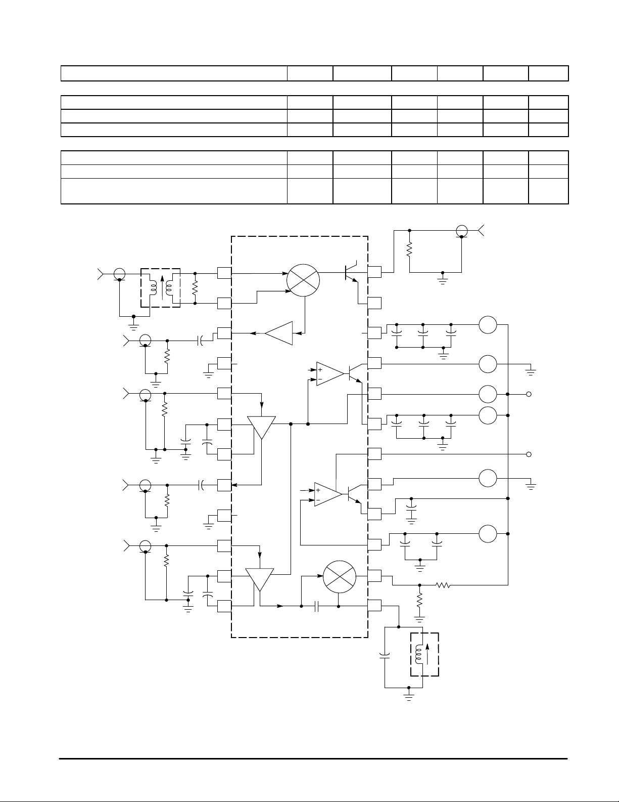
RF Input
130MHz
Mixer
Output
IF Input
IF Output
Limiter
Input
SMA
(1)
1:4
TR 1
330
50
1.0 n
330
50
1.0 n
200
1.0 n
1.0 n
1.0 n
10
11
1.0 n
12
1
2
3
4
5
6
7
8
9
Figure 1. T est Circuit
MC13156
Mixer
V
CC
V
CC
LIM Amp
Bias
IF Amp
Bias
Data
Slicer
5.0 p
Local
Oscillator
1.0
1.0
µ
µ
Input
140.7MHz
200m Vrms
A
A
A
A
A
V
Carrier
Detect
V
EE
Data Slicer
Hold
50
24
23
22
V
EE
V
V
EE
EE
21
20
19
18
17
16
15
14
13
100 n
RSSI
Output
100 n
Data Output
1.0 n
1.0 n
1.0 n
100 k
100 k
+
+
1.0 n100 n
NOTES: 1. TR 1 Coilcraft 1:4 impedance transformer.
2.VCC is DC Ground.
3.1.5 µH variable shielded inductor:
T oko Part # 292SNS–T1373 or Equivalent.
MOTOROLA RF/IF DEVICE DATA
150 p
(3)
1.0 µH
3

MC13156
DOCUMENT CONTAINS SCANNED IMAGES WHICH
COULD NOT BE PROCESSED FOR PDF FILES. FOR
COMPLETE DOCUMENT WITH IMAGES PLEASE
ORDER FROM MFAX OR THE LITERATURE
DISTRIBUTION CENTER
4
MOTOROLA RF/IF DEVICE DATA
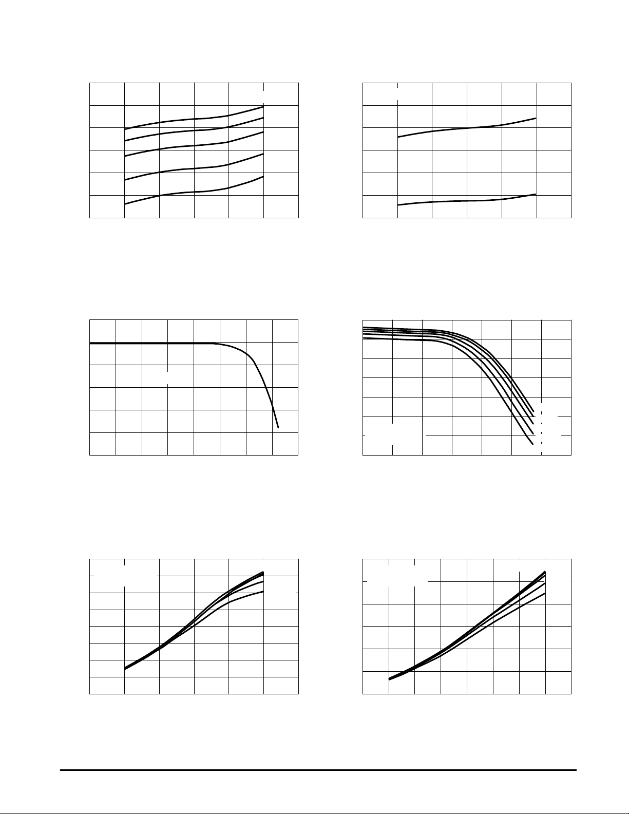
Figure 2. Total Drain Current versus Supply
V oltage and Temperature
6.5
(mA)
6.0
TOTAL
I
5.5
5.0
4.5
4.0
TOTAL DRAIN CURRENT,
3.5
1.0
2.0 3.0 4.0 5.0 6.0 7.0
VEE, SUPPLY VOLTAGE (–Vdc)
Figure 4. Mixer Gain versus Input Signal Level
25.0
TA = 85°C
55°C
25°C
–10°C
–40°C
MC13156
Figure 3. Drain Currents versus Supply V oltage
4.0
TA = 25°C
3.6
3.2
2.8
2.4
DRAIN CURRENTS (mA)
22
I
,
2.0
19
I
1.6
1.0 2.0 3.0 4.0 5.0 6.0 7.0
VEE, SUPPLY VOLTAGE (–Vdc)
I
22
I
19
Figure 5. IF Amplifier Gain versus Input
Signal Level and Ambient T emperature
40
22.5
20.0
TA = 25°C
17.5
15.0
MIXER GAIN (dB)
12.5
10.0
–90
–80 –70 –60 –50 –40 –30 –20 –10
Pin, RF INPUT SIGNAL LEVEL (dBm)
Figure 6. IF Amplifier RSSI Output Current versus
Input Signal Level and Ambient T emperature
µ
IF AMPLIFIER RSSI CURRENT ( A)
20.0
17.5
15.0
12.5
10.0
7.5
5.0
2.5
–50
0
VEE = –5.0 Vdc
f = 10.7 MHz
–40 –30 –20 –10 0 10
Pin, IF INPUT SIGNAL LEVEL (dBm)
TA = 25° to 85°C
–10°C
–40°C
38
36
34
32
30
IF AMPLIFIER GAIN (dB)
VEE = –5.0 Vdc
28
f = 10.7 MHz
26
–65
–60 –55 –50 –45 –40 –35 –30
Pin, IF INPUT SIGNAL LEVEL (dBm)
Figure 7. Limiter Amplifier RSSI Output Current
versus Input Signal Level and T emperature
µ
30
VEE = – 5.0 Vdc
f = 10.7 MHz
25
20
15
10
5.0
0
–70
LIMITER AMPLIFIER RSSI OUTPUT CURRENT ( A)
–60 –50 –40 –30 –20 –10 0 10
Pin, INPUT SIGNAL LEVEL (dBm)
TA = 25° to 85°C
85°C
55°C
25°C
–10°C
–40°C
–10°C
–40°C
MOTOROLA RF/IF DEVICE DATA
5
MC13156
32 k
32 k
290
Detect
Carrier
out
IF
8
Figure 8.
Output
21
RSSI
Out
20
µ
400
µ
28
Demod
14
17
DS
Output
in
DS
15
Gnd
DS
16
DSHold
18
64 k64 k
64 k
Data Slicer
16 k
1.4 k
5
7
6
dec1
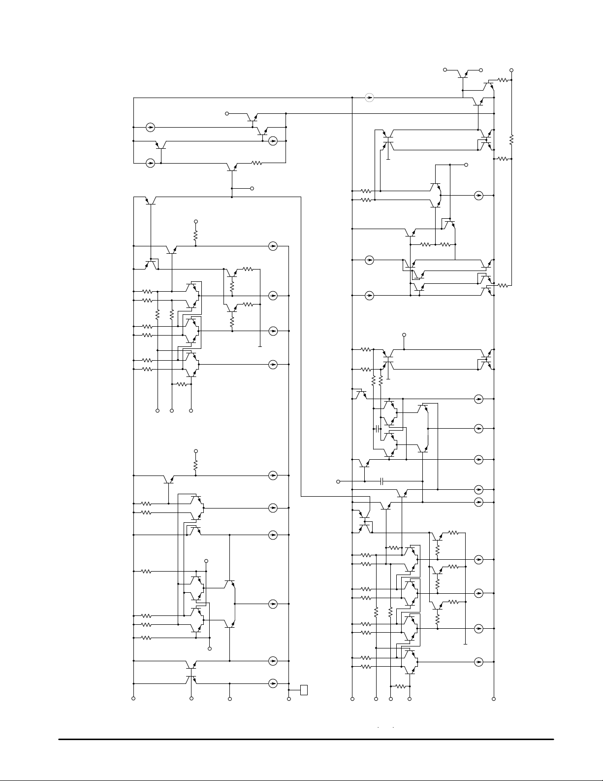
IF
Figure 8. MC13156DW Internal Circuit Schematic
1.0 k 1.0 k
dec2
IF
in
IF
Mix
330
Output
3
in2
RF
in1
RF
2
1
13
coil
Quad
5.0 p
Linear Amplifier Quadrature Detector
4
CC1
V
Local Oscillator Mixer IF Amplifier RSSI Carrier Detect
base
O
24
23
emitter
EE1
V
22
6
CC2
V
9
11
dec1IMdec2
IM
12
10
in
LIM
EE2
V
19
MOTOROLA RF/IF DEVICE DATA
 Loading...