

Motorola MC13155D Datasheet
The MC13155 is a complete wideband FM detector designed for satellite
TV and other wideband data and analog FM applications. This device may
be cascaded for higher IF gain and extended Receive Signal Strength
Indicator (RSSI) range.
• 12 MHz Video/Baseband Demodulator
• Ideal for Wideband Data and Analog FM Systems
• Limiter Output for Cascade Operation
• Low Drain Current: 7.0 mA
• Low Supply Voltage: 3.0 to 6.0 V
• Operates to 300 MHz
Order this document by MC13155/D
WIDEBAND FM IF
SEMICONDUCTOR
TECHNICAL DATA
MAXIMUM RATINGS
Rating Pin Symbol Value Unit
Power Supply Voltage 11, 14 VEE (max) 6.5 Vdc
Input Voltage 1, 16 V
Junction Temperature – T
Storage Temperature Range – T
NOTE: Devices should not be operated at or outside these values. The “Recommended
Operating Conditions” provide for actual device operation.
in
J
stg
1.0 Vrms
+150 °C
– 65 to +150 °C
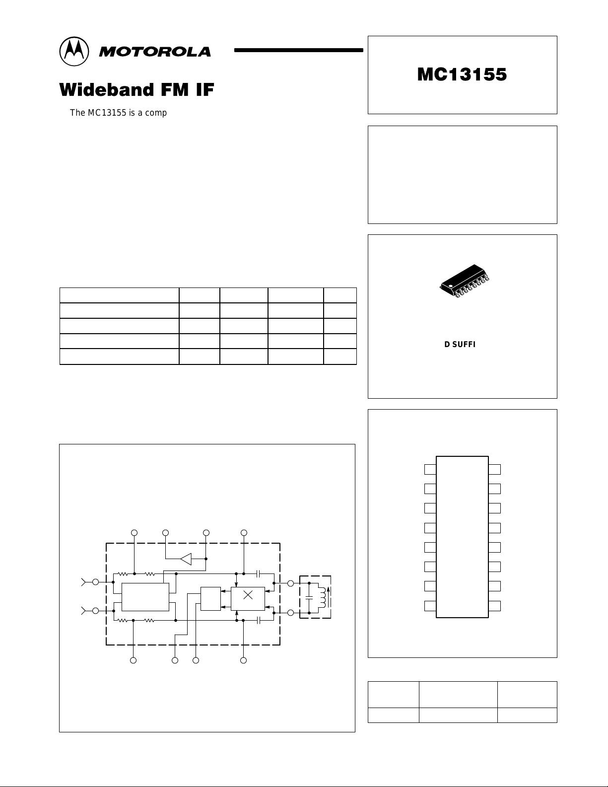
Figure 1. Representative Block Diagram
Buffered
Input
Input
16
RSSI
Decouple
1
Output
15
Three Stage
Amplifier
RSSI
Output
Limiter
Output
101213
9
Detector
8
Quad
Coil
Input
Decouple
VCC1
Output
Output
VCC2
Limiter Out
Quad Coil
16
1
D SUFFIX
PLASTIC PACKAGE
CASE 751B
(SO–16)
PIN CONNECTIONS
1
2
3
4
5
6
7
8
(Top View)
16
15
14
13
12
11
10
9
Input
Decouple
VEE1
RSSI Buffer
RSSI
VEE2
Limiter Out
Quad Coil
7542
Decouple
NOTE: This device requires careful layout and decoupling to ensure stable operation.
Balanced
Outputs
Limiter
Output
MOTOROLA ANALOG IC DEVICE DATA
ORDERING INFORMATION
Operating
Device
MC13155D TA = – 40 to +85°C SO–16
Motorola, Inc. 1996 Rev 1
Temperature Range
Package
1
MC13155
RECOMMENDED OPERATING CONDITIONS
Rating Pin Symbol Value Unit
Power Supply Voltage (TA= 25°C) 11, 14 V
–40°C ≤ TA ≤ 85°C 3, 6 V
Maximum Input Frequency 1, 16 f
Ambient Temperature Range – T
EE
CC
in
J
– 3.0 to – 6.0 Vdc
Grounded
300 MHz
– 40 to + 85 °C
DC ELECTRICAL CHARACTERISTICS (T
Characteristic
Drain Current 11 I
(VEE = – 5.0 Vdc) 14 I
(VEE = – 5.0 Vdc) 14 I
Drain Current Total (see Figure 3) 11, 14 I
(VEE = – 5.0 Vdc) 5.0 7.5 10.5
(VEE = – 6.0 Vdc) 5.0 7.5 10.5
(VEE = – 3.0 Vdc) 4.7 6.6 9.5
AC ELECTRICAL CHARACTERISTICS (T
Characteristic
Input for – 3 dB Limiting Sensitivity 1, 16 – 1.0 2.0 mVrms
Differential Detector Output Voltage (Vin = 10 mVrms) 4, 5 mV
(f
= ± 3.0 MHz) (VEE = – 6.0 Vdc) 470 590 700
dev
Detector DC Offset Voltage 4, 5 –250 – 250 mVdc
RSSI Slope 13 1.4 2.1 2.8 µA/dB
RSSI Dynamic Range 13 31 35 39 dB
RSSI Output 12 µA
(Vin = 100 µVrms) – 2.1 –
(Vin = 1.0 mVrms) – 2.4 –
(Vin = 10 mVrms) 16 24 36
(Vin = 100 mVrms) – 65 –
(Vin = 500 mVrms) – 75 –
RSSI Buffer Maximum Output Current (Vin = 10 mVrms) 13 – 2.3 – mAdc
Differential Limiter Output mVrms
(Vin = 1.0 mVrms) 7, 10 100 140 –
(Vin = 10 mVrms) – 180 –
Demodulator Video 3.0 dB Bandwidth 4, 5 – 12 – MHz
Input Impedance (Figure 14) 1, 16
@ 70 MHz Rp (VEE = – 5.0 Vdc) – 450 – Ω
@ 70 MHz Cp (C2=C15 = 100 p) – 4.8 – pF
Differential IF Power Gain 1, 7, 10, 16 – 46 – dB
NOTE: Positive currents are out of the pins of the device.
(VEE = – 5.0 Vdc) 450 570 680
(VEE = – 3.0 Vdc) 380 500 620
= 25°C, no input signal.)
A
Pin Symbol Min Typ Max Unit
11
14
14
Total
= 25°C, fIF = 70 MHz, VEE = – 5.0 Vdc Figure 2, unless otherwise noted.)
A
2.0 2.8 4.0 mA
3.0 4.3 6.0
3.0 4.3 6.0
5.0 7.1 10 mA
Pin Min Typ Max Unit
p–p
2
MOTOROLA ANALOG IC DEVICE DATA
MC13155
CIRCUIT DESCRIPTION
The MC13155 consists of a wideband three–stage limiting
amplifier, a wideband quadrature detector which may be
operated up to 200 MHz, and a received signal strength
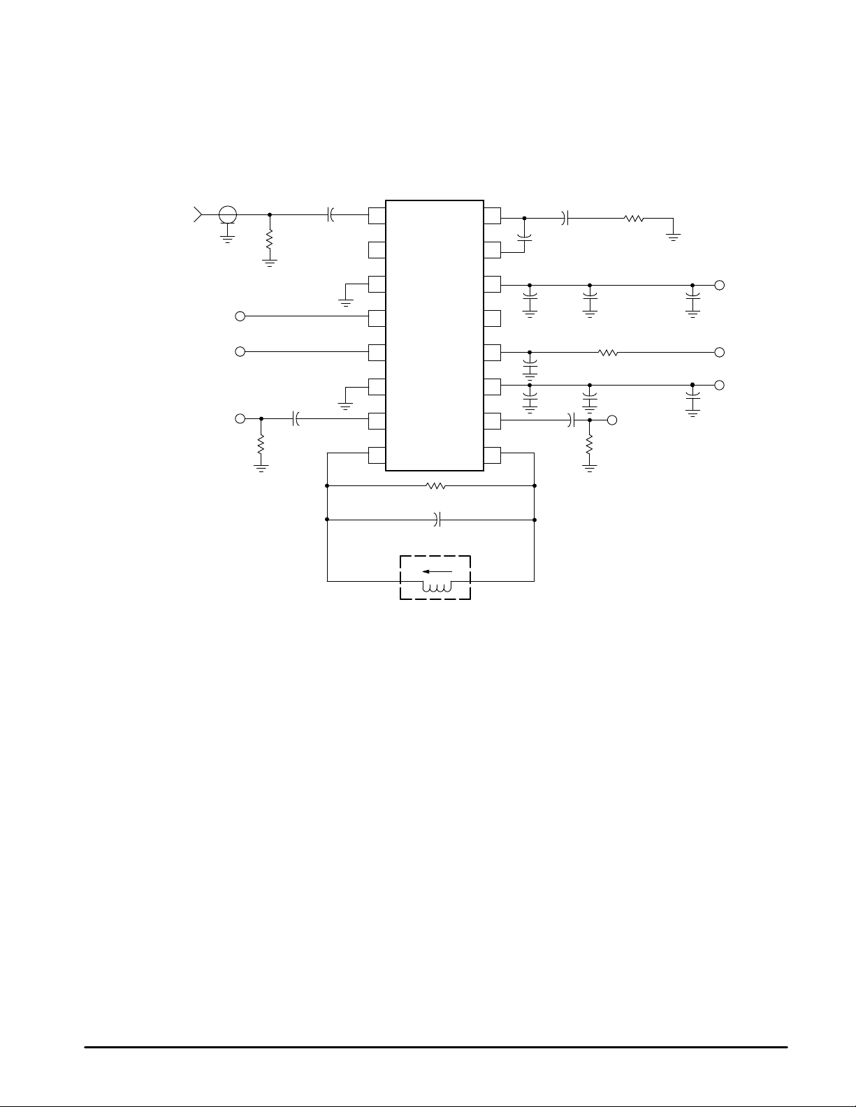
Figure 2. T est Circuit
1.0n
V
in
Video
Output
Limiter 1
Output
49.9
1.0n
330
1
2
3
4
5
6
7
8
IN1
DEC1
VCC1
DETO1
DETO2
VCC2
LIMO1
indicator (RSSI) circuit which provides a current output
linearly proportional to the IF input signal level for
approximately 35 dB range of input level.
IN2
DEC2
VEE1
RSSI
Buffer
RSSI
VEE2
LIMO2
QUAD2QUAD1
16
15
14
13
12
11
10
1.0n
10n
1.0n
1.0n
1.0n
1.0n
9
100n
1.0k
100n
330
27
Limiter 2
Output
10
10
V
µ
µ
EE
+
V
EE
V
EE
+
APPLICATIONS INFORMATION
Evaluation PC Board
The evaluation PCB shown in Figures 19 and 20 is very
versatile and is designed to cascade two ICs. The center
section of the board provides an area for attaching all surface
mount components to the circuit side and radial leaded
components to the component ground side of the PCB (see
Figures 17 and 18). Additionally, the peripheral area
surrounding the RF core provides pads to add supporting
and interface circuitry as a particular application dictates.
This evaluation board will be discussed and referenced in
this section.
Limiting Amplifier
Differential input and output ports interfacing the three
stage limiting amplifier provide a differential power gain of
typically 46 dB and useable frequency range of 300 MHz.
The IF gain flatness may be controlled by decoupling of the
internal feedback network at Pins 2 and 15.
499
20p
L1
260n
L1 – Coilcraft part number 146–09J08S
Scattering parameter (S–parameter) characterization of
the IF as a two port linear amplifier is useful to implement
maximum stable power gain, input matching, and stability
over a desired bandpass response and to ensure stable
operation outside the bandpass as well. The MC13155 is
unconditionally stable over most of its useful operating
frequency range; however, it can be made unconditionally
stable over its entire operating range with the proper
decoupling of Pins 2 and 15. Relatively small decoupling
capacitors of about 100 pF have a significant effect on the
wideband response and stability. This is shown in the
scattering parameter tables where S–parameters are shown
for various values of C2 and C15 and at VEE of – 3.0 and
– 5.0 Vdc.
MOTOROLA ANALOG IC DEVICE DATA
3

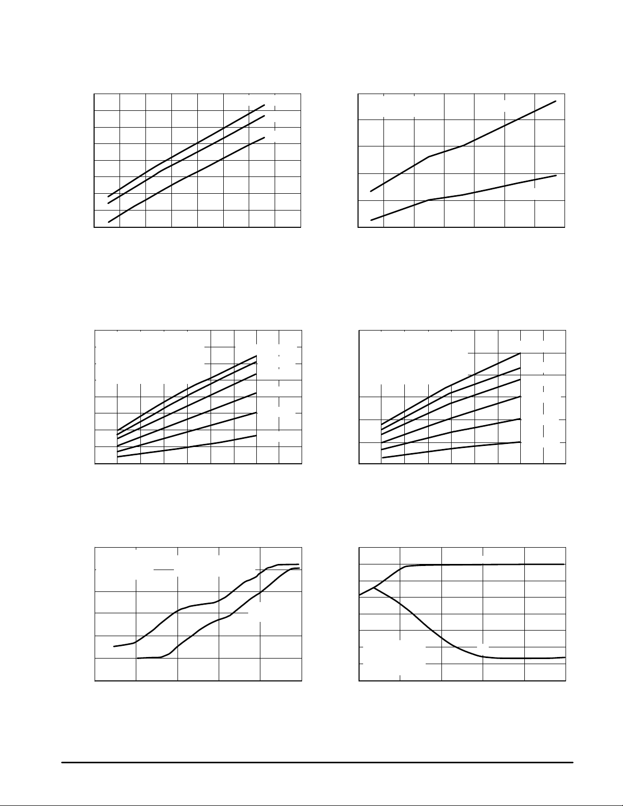
TYPICAL PERFORMANCE AT TEMPERATURE
Figure 3. Drain Current versus Supply Voltage
10
TA = 25°C
8.0
6.0
4.0
, DRAIN CURRENT (mAdc)
Total
2.0
and I
14
I
0.0
0.0
1.0 2.0 3.0 4.0 5.0 6.0 7.0 8.0 100 1000
I
= I14 + I
Total
VEE, SUPPLY VOLTAGE (–Vdc)
11
I
14
MC13155
(See Figure 2. T est Circuit)
Figure 4. RSSI Output versus Frequency and
100
80
µ
60
40
RSSI OUTPUT ( A)
12
I ,
20
0
10
Input Signal Level
VEE = – 5.0Vdc
0 dBm
–10 dBm
– 20 dBm
– 30 dBm
– 40 dBm
f, FREQUENCY (MHz)
Figure 5. T otal Drain Current versus Ambient
T emperature and Supply Voltage
8.5
8.0
7.5
7.0
6.5
TOTAL DRAIN CURRENT (mAdc)
6.0
14
5.5
and I ,
11
5.0
I
–50 – 30 –10 10 30 50 70 90 110 –50 – 30 –10 10 30 50 70 90 110
TA, AMBIENT TEMPERATURE (°C)
VEE = – 6.0 Vdc
– 3.0 Vdc
– 5.0 Vdc
Figure 7. RSSI Output versus Ambient
T emperature and Supply Voltage
µ
RSSI OUTPUT ( A)
12
I ,
25.0
24.5
24.0
23.5
23.0
22.5
22.0
VEE = – 6.0 Vdc
VEE = – 5.0 Vdc
VEE = – 3.0 Vdc
Figure 6. Detector Drain Current and Limiter
Drain Current versus Ambient Temperature
5.59.0
f = 70 MHz
5.0
VEE = – 5.0 Vdc
4.5
4.0
3.5
DRAIN CURRENT (mAdc)
3.0
11
2.5
14
I and I ,
2.0
TA, AMBIENT TEMPERATURE (
Figure 8. RSSI Output versus Input Signal
V oltage (Vin at Temperature)
100
TA = + 85°C
µ
RSSI OUTPUT ( A)
12
I ,
80
60
40
20
I
14
I
11
°
C)
+25°C
–40°C
21.5
4
0
– 30 –10 10 30 50 70 90 110 1.0 10 100 1000
–50
0.1
Vin, INPUT VOLTAGE (mVrms)TA, AMBIENT TEMPERATURE (°C)
MOTOROLA ANALOG IC DEVICE DATA
MC13155
Figure 9. Differential Detector Output
V oltage versus Ambient Temperature
and Supply V oltage
750 220
700
650
600
pp
550
500
(Pins 4, 5), (mV )
450
400
DIFFERENTIAL DETECTOR OUTPUT VOLTAGE
350
–50 – 30 –10 10 30 50 70 90 110
VEE = – 6.0 Vdc
– 5.0 Vdc
– 3.0 Vdc
Figure 11A. Differential Detector Output Voltage
versus Q of Quadrature LC Tank
)
1600
Vin = – 30 dBm
pp
VEE = – 5.0 Vdc
1400
fc = 70 MHz
f
1200
1000
800
600
400
200
DIFFERENTIAL DETECTOR OUTPUT (mV
= 1.0 MHz
mod
(Figure 16 no external capacitors
between Pins 7, 8 and 9, 10)
0
1.5
2.5 3.5 4.5 5.5
2.0 3.0 4.0 5.0 6.0 1.5 2.5 3.5 4.5 5.52.0 3.0 4.0 5.0 6.0
Q OF QUADRATURE LC TANK
f
= ±6.0 MHz
dev
±
5.0 MHz
±
4.0 MHz
±
3.0 MHz
±
2.0 MHz
±
1.0 MHz
Figure 10. Differential Limiter Output Voltage
versus Ambient T emperature
(Vin = 1 and 10 mVrms)
f = 70 MHz
VEE = – 5.0 Vdc
200
180
160
(Pins 7, 10), (mVrms)
140
DIFFERENTIAL LIMITER OUTPUT VOLTAGE
120
–50 – 30 –10 10 30 50 70 90
TA, AMBIENT TEMPERATURE (°C)TA, AMBIENT TEMPERATURE (°C)
Vin = 10 mVrms
Vin = 1.0 mVrms
Figure 11B. Differential Detector Output Voltage
versus Q of Quadrature LC Tank
)
2400
Vin = – 30 dBm
pp
2000
1600
1200
800
400
0
DIFFERENTIAL DETECTOR OUTPUT (mV
VEE = – 5.0 Vdc
fc = 70 MHz
f
= 1.0 MHz
mod
(Figure 16 no external capacitors
between Pins 7, 8 and 9, 10)
Q OF QUADRATURE LC TANK
f
= ±6.0 MHz
dev
±
5.0 MHz
±
4.0 MHz
±
3.0 MHz
±
2.0 MHz
±
1.0 MHz
Figure 11.
Figure 12. RSSI Output V oltage versus IF Input
0
VEE = – 5.0 Vdc
fc = 70 MHz
–1.0
(See Figure 16)
–2.0
–3.0
–4.0
–5.0
RSSI OUTPUT VOLTAGE, (Vdc)
–80 –60 –40 –20 0 20
Capacitively coupled
interstage: no attenuation
15 dB Interstage
Attenuator
IF INPUT, (dBm)
MOTOROLA ANALOG IC DEVICE DATA
Figure 13. – S+N, N versus IF Input
10
0
–10
–20
–30
S+N, N (dB)
–40
fc = 70 MHz
–50
f
= 1.0 MHz
mod
±
5.0 MHz
f
=
dev
–60
VEE = – 5.0 Vdc
–70
–90 – 70 – 50 – 30 –10 10
IF INPUT (dBm)
S+N
N
5
 Loading...