

Motorola MC12439FN Datasheet
SEMICONDUCTOR TECHNICAL DATA
1
REV 3
Motorola, Inc. 1997
1/97
The MC12439 is a general purpose synthesized clock source targeting
applications that require both serial and parallel interfaces. Its internal
VCO will operate over a range of frequencies from 400 to 800MHz. The
differential PECL output can be configured to be the VCO frequency
divided by 1, 2, 4, or 8. With the output configured to divide the VCO
frequency by 1, and with a 16.66MHz external quartz crystal used to
provide the reference frequency, the output frequency can be specified in
16.66MHz steps.
• 50 to 800MHz Differential PECL Outputs
• ±25ps Typical Peak–to–Peak Output Jitter
• Minimal Frequency Over–Shoot
• Synthesized Architecture
• Serial 3–Wire Interface
• Parallel Interface for Power–Up
• Quartz Crystal Interface
• 28–Lead PLCC Package
• Operates from 3.3V or 5.0V Power Supply
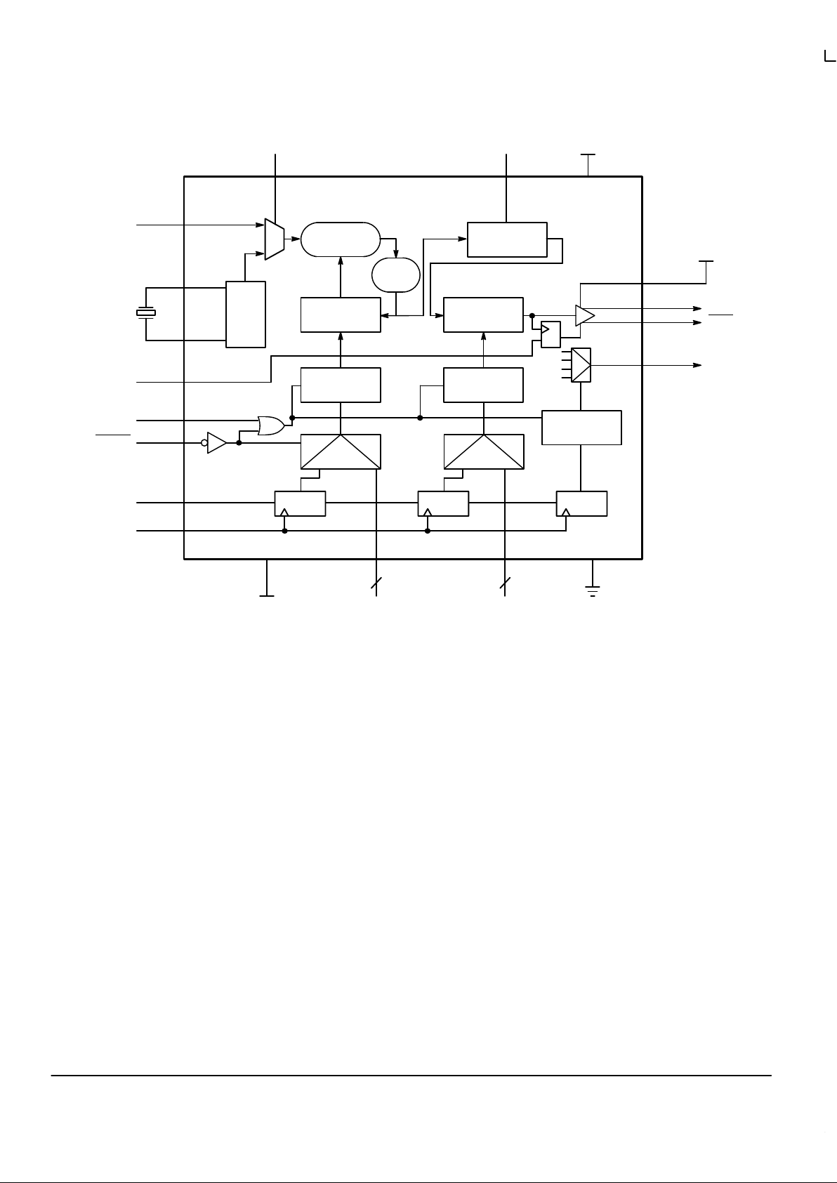
Functional Description
The internal oscillator uses the external quartz crystal as the basis of its frequency reference. The output of the reference
oscillator is sent directly to the phase detector. With a 16.66MHz crystal, this provides a reference frequency of 16.66MHz.
Although this data sheet illustrates functionality only for a 16MHz and 16.66MHz crystal, any crystal in the 10–20MHz range can
be used. In addition to the crystal, an LVCMOS input can also be used as the PLL reference. The reference is selected via the
XTAL_SEL input pin.
The VCO within the PLL operates over a range of 400 to 800MHz. Its output is scaled by a divider that is configured by either
the serial or parallel interfaces. The output of this loop divider is also applied to the phase detector.
The phase detector and loop filter attempt to force the VCO output frequency to be M times the reference frequency by
adjusting the VCO control voltage. Note that for some values of M (either too high or too low) the PLL will not achieve loop lock.
The output of the VCO is also passed through an output divider before being sent to the PECL output driver. This output divider
is configured through either the serial or the parallel interfaces, and can provide one of four division ratios (1, 2, 4, or 8). This
divider extends performance of the part while providing a 50% duty cycle.
The output driver is driven differentially from the output divider, and is capable of driving a pair of transmission lines terminated
in 50Ω to VCC – 2.0.
The configuration logic has two sections: serial and parallel. The parallel interface uses the values at the M[6:0] and N[1:0]
inputs to configure the internal counters. Normally, on system reset, the P_LOAD
input is held LOW until sometime after power
becomes valid. On the LOW–to–HIGH transition of P_LOAD
, the parallel inputs are captured. The parallel interface has priority
over the serial interface. Internal pullup resistors are provided on the M[6:0] and N[1:0] inputs to reduce component count in the
application of the chip.
The serial interface centers on a twelve bit shift register. The shift register shifts once per rising edge of the S_CLOCK input.
The serial input S_DATA must meet setup and hold timing as specified in the AC Characteristics section of this document. The
configuration latches will capture the value of the shift register on the HIGH–to–LOW edge of the S_LOAD input. See the
programming section for more information.
The TEST output reflects various internal node values, and is controlled by the T[2:0] bits in the serial data stream. See the
programming section for more information.
The PWR_DOWN pin, when asserted, will synchronously divide the FOUT by 16. The power down sequence is clocked by the
PLL reference clock, thereby causing the frequency reduction to happen relatively slowly. Upon de–assertion of the
PWR_DOWN pin, the FOUT input will step back up to its programmed frequency in four discrete increments.
HIGH FREQUENCY PLL
CLOCK GENERATOR
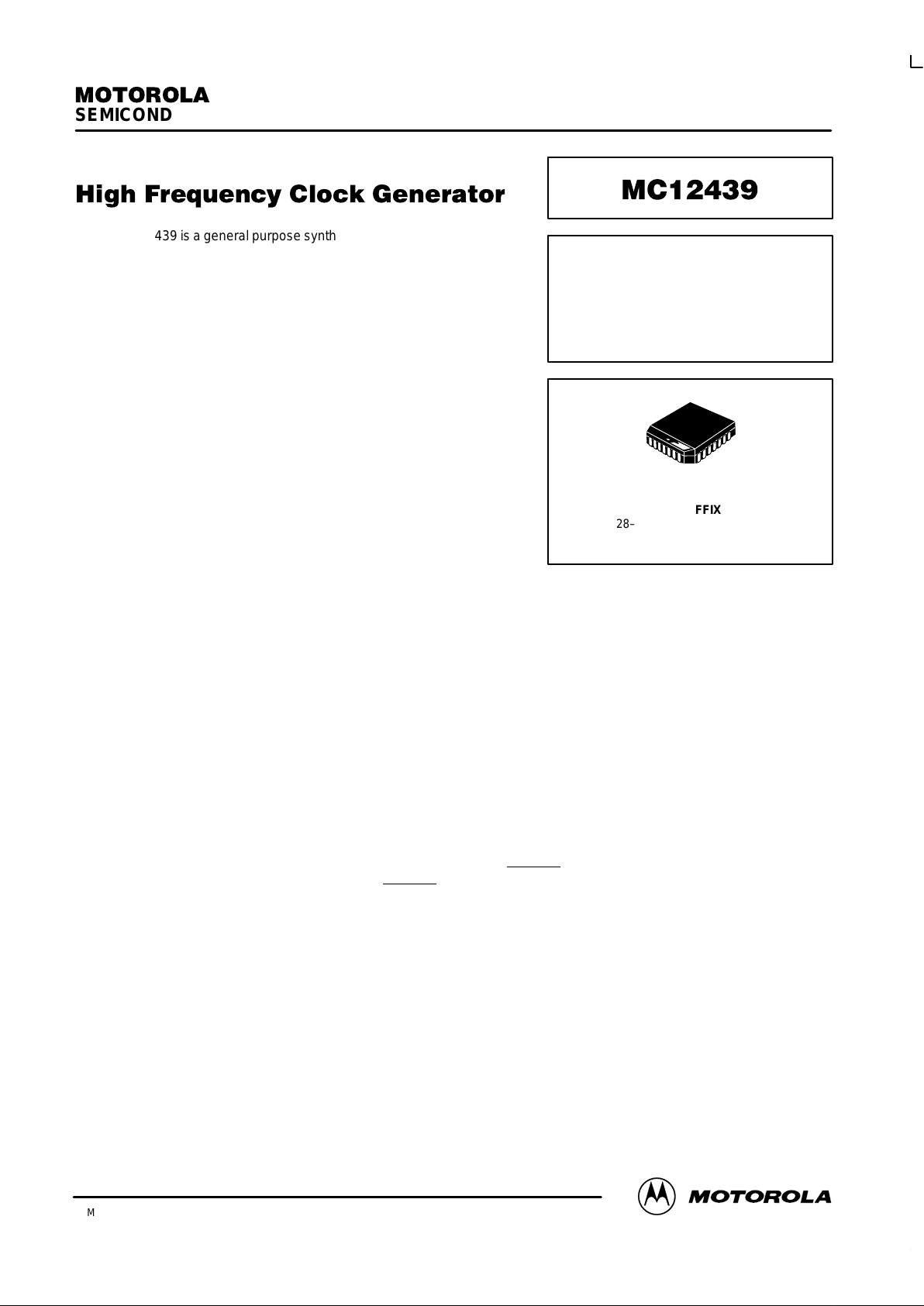
FN SUFFIX
28–LEAD PLCC PACKAGE
CASE 776–02
MC12439
MOTOROLA TIMING SOLUTIONS
BR1333 — Rev 6
2
1
N[1]
N[0]
NC
XTAL_SEL
M[6]
M[5]
M[4]XTAL1
FREF_EXT
PWR_DOWN
PLL–V
CC
S_LOAD
S_DATA
S_CLOCK
4
3
2
28
27
26
25
24
23
22
21
20
19
18
17
16
15
14
13
12
11109
7
8
6
5
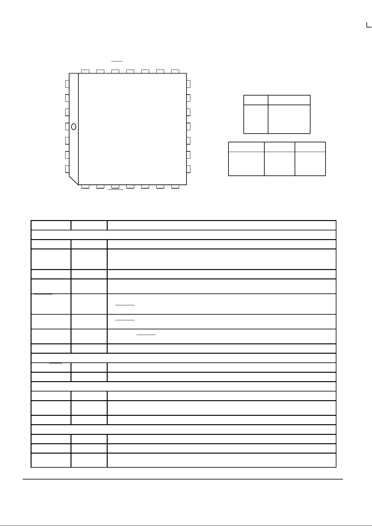
Figure 1. 28–Lead Pinout (Top View)
P_LOAD
VCCFOUT FOUT GND V
CC
TEST GND
M[3]M[2]M[1]M[0]
OE
XTAL2
N[1:0]
0 0
0 1
1 0
1 1
Output Division
2
4
8
1
Input
PWR_DOWN
XTAL_SEL
OE
0
FOUT
FREF_EXT
Disabled
1
FOUT/16
XTAL
Enabled
PIN DESCRIPTIONS
Pin Name Type Function
Inputs
XTAL1, XTAL2 — These pins form an oscillator when connected to an external series–resonant crystal.
S_LOAD Int. Pulldown This pin loads the configuration latches with the contents of the shift registers. The latches will be
transparent when this signal is HIGH, thus the data must be stable on the HIGH–to–LOW transition of
S_LOAD for proper operation.
S_DATA Int. Pulldown This pin acts as the data input to the serial configuration shift registers.
S_CLOCK Int. Pulldown This pin serves to clock the serial configuration shift registers. Data from S_DAT A is sampled on the rising
edge.
P_LOAD Int. Pullup This pin loads the configuration latches with the contents of the parallel inputs .The latches will be
transparent when this signal is LOW, thus the parallel data must be stable on the LOW–to–HIGH transition
of P_LOAD
for proper operation.
M[6:0] Int. Pullup These pins are used to configure the PLL loop divider. They are sampled on the LOW–to–HIGH transition
of P_LOAD
. M[6] is the MSB, M[0] is the LSB.
N[1:0] Int. Pullup These pins are used to configure the output divider modulus. They are sampled on the LOW–to–HIGH
transition of P_LOAD
.
OE Int. Pullup Active HIGH Output Enable.
Outputs
F
OUT
, F
OUT
— These differential positive–referenced ECL signals (PECL) are the output of the synthesizer.
TEST — The function of this output is determined by the serial configuration bits T[2:0].
Power
V
CC
— This is the positive supply for the chip, and is connected to +3.3V or 5.0V (VCC = PLL_VCC).
PLL_V
CC
— This is the positive supply for the PLL, and should be as noise–free as possible for low–jitter operation. This
supply is connected to +3.3V or 5.0V (VCC = PLL_VCC).
GND — These pins are the negative supply for the chip and are normally all connected to ground.
Other
PWR_DOWN Int. Pulldown LVCMOS input that forces the FOUT output to synchronously reduce its frequency by a factor of 16.
FREF_EXT Int. Pulldown LVCMOS input which can be used as the PLL reference frequency.
XTAL_SEL Int. Pullup LVCMOS input that selects between the XTAL and FREF_EXT PLL reference inputs. A HIGH selects the
XTAL input.
MC12439
TIMING SOLUTIONS
BR1333 — Rev 6
3 MOTOROLA
Figure 2. MC12439 Block Diagram
16.66MHz
S_LOAD
P_LOAD
S_DATA
S_CLOCK
XTAL1
XTAL2
OSC
4
5
PHASE
DETECTOR
28
7
7–BIT DIV M
COUNTER
LATCH
VCO
DIV N
(1, 2, 4, 8)
LATCH
400–800
MHz
FOUT
FOUT
+3.3 or 5.0V
25
24
23
V
CC0
LATCH
TEST
20
+3.3 or 5.0V
PLL_V
CC
01
7–BIT SR
27
26
01
2–BIT SR 3–BIT SR
V
CC1
+3.3 or 5.0V
M[6:0]
7
8
→
14
N[1:0]
2
17, 1821 22, 19
OE
6
FREF_EXT
3
0
1
XTAL_SEL
15
PWR_DOWN
2
POWER DOWN
PROGRAMMING INTERF ACE
Programming the device amounts to properly configuring
the internal dividers to produce the desired frequency at the
outputs. The output frequency can by represented by this
formula:
FOUT = F
XTAL
x M ÷ N (1)
Where F
XTAL
is the crystal frequency, M is the loop divider
modulus, and N is the output divider modulus. Note that it is
possible to select values of M such that the PLL is unable to
achieve loop lock. To avoid this, always make sure that M is
selected to be 25 ≤ M ≤ 50 for a 16MHz input reference.
For input references other than 16MHz, the valid M values
can be calculated from the valid VCO range of 400–800MHz.
Assuming that a 16MHz reference frequency is used the
above equation reduces to:
FOUT = 16 x M ÷ N
Substituting the four values for N (1, 2, 4, 8) yields:
FOUT = 16M, FOUT = 8M,
FOUT = 4M and FOUT = 2M
for 25 < M < 50
The user can identify the proper M and N values for the
desired frequency from the above equations. The four output
frequency ranges established by N are 400–800MHz,
200–400MHz, 100–200MHz and 50–100MHz respectively.
From these ranges the user will establish the value of N
required, then the value of M can be calculated based on the
appropriate equation above. For example if an output
frequency of 384MHz was desired the following steps would
be taken to identify the appropriate M and N values. 384MHz
falls within the frequency range set by an N value of 2 so N
[1:0] = 00. For N = 2 FOUT = 8M and M = FOUT ÷ 8.
Therefore M = 384 ÷ 8 = 48, so M[8:0] = 0110000.
For input reference frequencies other than 16MHz the set
of appropriate equations can be deduced from equation 1.
For computer applications another useful frequency base
would be 16.666MHz. From this reference one can generate
a family of output frequencies at multiples of the 33.333MHz
PCI clock. As an example to generate a 533.333MHz clock
MC12439
MOTOROLA TIMING SOLUTIONS
BR1333 — Rev 6
4
from a 16.666MHz reference the following M and N values
would be used:
FOUT = 16.666 x M ÷ N
Let N = 1, M = 533.333 ÷ 16.666 = 32
The value for M falls within the constraints set for PLL stability
(400÷16.666 ≤ M ≤ 800÷16.666; 24 ≤ M ≤ 48), therefore
N[1:0] = 11 and M[6:0} = 0100000. If the value for M fell
outside of the valid range a different N value would be
selected to try to move M in the appropriate direction.
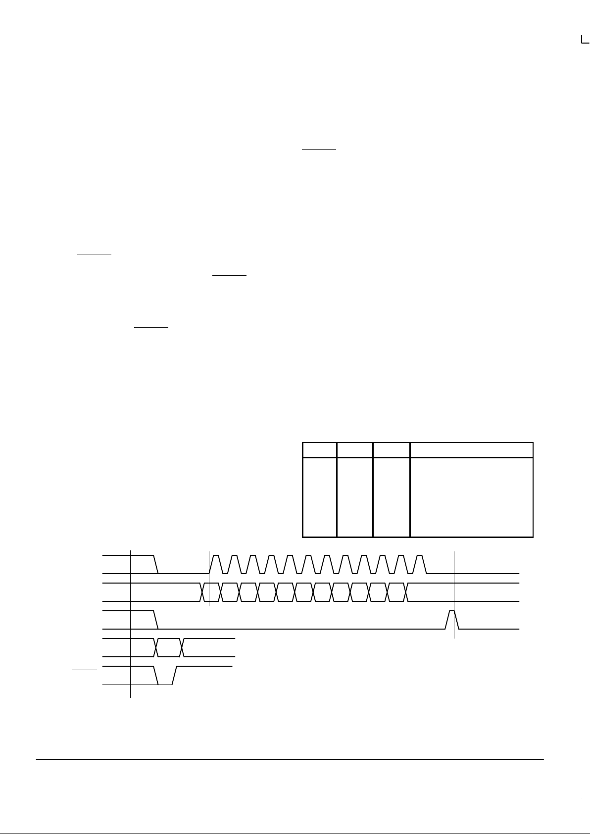
The M and N counters can be loaded either through a
parallel or serial interface. The parallel interface is controlled
via the P_LOAD
signal such that a LOW to HIGH transition
will latch the information present on the M[6:0] and N[1:0]
inputs into the M and N counters. When the P_LOAD
signal is
LOW the input latches will be transparent and any changes
on the M[6:0] and N[1:0] inputs will affect the FOUT output
pair. To use the serial port the S_CLOCK signal samples the
information on the S_DA TA line and loads it into a 12 bit shift
register. Note that the P_LOAD
signal must be HIGH for the
serial load operation to function. The Test register is loaded
with the first three bits, the N register with the next two and
the M register with the final eight bits of the data streeam on
the S_DATA input. For each register the most significant bit is
loaded first (T2, N1 and M6). A pulse on the S_LOAD pin
after the shift register is fully loaded will transfer the divide
values into the counters. The HIGH to LOW transition on the
S_LOAD input will latch the new divide values into the
counters. NO TAG illustrates the timing diagram for both a
parallel and a serial load of the MC12439 synthesizer.
M[6:0] and N[1:0] are normally specified once at power–up
through the parallel interface, and then possibly again
through the serial interface. This approach allows the
application to come up at one frequency and then change or
fine–tune the clock as the ability to control the serial interface
becomes available.
The TEST output provides visibility for one of the several
internal nodes as determined by the T[2:0] bits in the serial
configuration stream. It is not configurable through the
parallel interface. Although it is possible to select the node
that represents FOUT, the CMOS output may not be able to
toggle fast enough for some of the higher output frequencies.
The T2, T1 and T0 control bits are preset to ‘000’ when
P_LOAD
is LOW so that the PECL FOUT outputs are as
jitter–free as possible. Any active signal on the TEST output
pin will have detrimental affects on the jitter of the PECL
output pair. In normal operations, jitter specifications are only
guaranteed if the TEST output is static. The serial
configuration port can be used to select one of the alternate
functions for this pin.
Most of the signals available on the TEST output pin are
useful only for performance verification of the MC12439
itself. However the PLL bypass mode may be of interest at
the board level for functional debug. When T[2:0] is set to 110
the MC12439 is placed in PLL bypass mode. In this mode the
S_CLOCK input is fed directly into the M and N dividers. The
N divider drives the FOUT differential pair and the M counter
drives the TEST output pin. In this mode the S_CLOCK input
could be used for low speed board level functional test or
debug. Bypassing the PLL and driving FOUT directly gives
the user more control on the test clocks sent through the
clock tree. NO TAG shows the functional setup of the PLL
bypass mode. Because the S_CLOCK is a CMOS level the
input frequency is limited to 250MHz or less. This means the
fastest the FOUT pin can be toggled via the S_CLOCK is
250MHz as the minimum divide ratio of the N counter is 1.
Note that the M counter output on the TEST output will not be
a 50% duty cycle due to the way the divider is implemented.
T2 T1 T0 TEST (Pin 20)
0
0
0
0
1
1
1
1
0
0
1
1
0
0
1
1
0
1
0
1
0
1
0
1
SHIFT REGISTER OUT
HIGH
FREF
M COUNTER OUT
FOUT
LOW
PLL BYPASS
FOUT/4
Figure 3. Timing Diagram
S_CLOCK
S_DATA
S_LOAD
M[6:0]
N[1:0]
P_LOAD
T2 T1 T0 N1 N0 M6 M5 M4 M3 M2 M1
M0
M, N
First
Bit
Last
Bit
 Loading...