

Motorola MC12181D Datasheet
The MC12181 is a monolithic bipolar synthesizer integrating a high
performance prescaler, programmable divider, phase/frequency detector,
charge pump, and reference oscillator/buffer functions. The device is
capable of synthesizing a signal which is 25 to 40 times the input reference
signal. The device has a 4–bit parallel interface to set the proper total
multiplication which can range from 25 to 40. When combined with an
external passive loop filter and VCO, the MC12181 serves as a complete
PLL subsystem.
• 2.7 to 5.5 V Operation
• Low power supply current of 4.25 mA typical
• On chip reference oscillator/buffer supporting wide frequency operating
range from 5 to 25 MHz
• 4–bit parallel interface for programming divider (N = 25 .... 40)
• Wide 125 – 1000 MHz frequency of operation
• Digital phase/frequency detector with linear transfer function
• Balanced Charge Pump Output
• Space efficient 16 lead SOIC package
• Operating Temperature Range of –40 to 85°C
• > 1000 V ESD Protection (I/O to Ground, I/O to V
The device is suitable for applications where a fixed local oscillator (LO)
needs to be synthesized or where a limited number of LO frequencies need
to be generated. The device also has auxiliary open emitter outputs (Pout
and Rout) for observing the inputs to the phase detector for verification
purposes. In normal use the pins should be left open. The Reset input is
normally LOW. When this input is placed in the HIGH state the reference
prescaler is reset and the charge pump output (Do) is placed in the OFF
state.
The 4–bit programming interface maps into divider states ranging from 25
to 40. A is the LSB and D is the MSB. The data inputs (A,B,C, and D) are
CMOS compatible and have pull–up resistors. The inputs can be tied directly
to Vcc or Ground for programming or can be interfaced to an external data
latch/register. Table 1 below has a mapping of the programming states.
T able 1. Programming States
D C B A Divider
L L L L 25
L L L H 26
L L H L 27
L L H H 28
L H L L 29
L H L H 30
L H H L 31
L H H H 32
H L L L 33
H L L H 34
H L H L 35
H L H H 36
H H L L 37
H H L H 38
H H H L 39
H H H H 40
CC
)
Order this document by MC12181/D
125 – 1000 MHZ
FREQUENCY SYNTHESIZER
SEMICONDUCTOR
TECHNICAL DATA
16
1
D SUFFIX
PLASTIC PACKAGE
CASE 751B
(SO–16)
PIN CONNECTIONS
AOSCin
161
BOSCout
152
CV
P
CC
(Top View)
ORDERING INFORMATION
Operating
Device
MC12181D TA = –40° to +85°C SO–16
Temperature Range
143
134
125
116
107
98
DV
PoutDo
ResetGND
RoutFin
GNDFin
Package
Motorola, Inc. 1997 Rev 2
MC12181
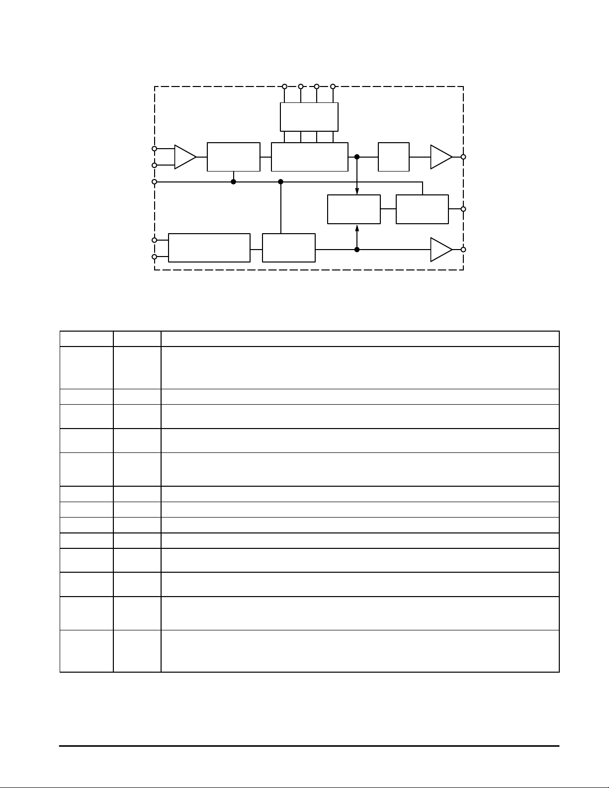
Figure 1. MC12181 Programmable Synthesizer
ABCD
DECODE
LOGIC
Fin
Fin
Reset
OSCin
OSCout
DIVIDE BY 8
PRESCALER
CRYSTAL
OSCILLA T OR/BUFFER
PROGRAMMABLE
DIVIDER (25 – 40)
DIVIDE BY 8
PRESCALER
PHASE/FREQ
DETECTOR
DIVIDE
BY 2
CHARGE
PUMP
Pout
Do
Rout
PIN NAMES
Pin No. Pin Function
1 OSCin An external parallel resonant, fundamental crystal is connected between OSCin and OSCout to form an internal
2 OSCout Oscillator output, for use with an external crystal as shown in Figure 2.
3 V
4 V
5 Do Single ended phase/frequency detector output. Three–state current sink/source output for use as a loop error
6 GND Ground. This pin should be directly tied to the ground plane.
7 Fin Prescaler input – The VCO signal is ac–coupled into the Fin Pin.
8 Fin Complementary prescaler input – This pin should be capacitively coupled to ground.
9 GND Ground. This pin should be directly tied to the ground plane.
10 Rout Open emitter test point used to verify proper operation of the reference divider chain. In normal operation this pin
11 Reset Test pin used to clear the prescalers (Reset = H). When the Reset is in the HIGH state, the charge pump output
12 Pout Open emitter test point used to verify proper operation of the programmable divider chain. The output is a
13
14
15
16
CC
D
C
B
A
reference crystal oscillator. External capacitors C1 and C2 are required to set the proper crystal load capacitance
and oscillator frequency (Figure 2). For an external reference oscillator, a signal is ac–coupled into the OSCin pin.
In either mode a 50 kΩ resistor MUST be connected between OSCin and OSCout.
Positive power supply for charge pump. VP MUST be greater than or equal to VCC. Bypassing should be placed
P
as close as possible to this pin and be connected directly to the ground plane.
Positive power supply. Bypassing should be placed as close as possible to this pin and be connected directly to
the ground plane.
signal when combined with an external low pass filter. The phase/frequency detector is characterized by a linear
transfer function.
should be left OPEN.
is disabled. The Reset input has an internal pulldown. In normal operation it can be left open or tied to ground.
divide–by–2 version of the programmable input to the phase/frequency detector. In normal operation this pin
should be left OPEN.
Digital control inputs for setting the value of the programmable divider. A is the LSB and D is the MSB. In normal
operation these pins can be tied to VCC and/or ground to program a fixed divide or they can be driven by a CMOS
logic level when used in a programmable mode. There is an internal pull–up resistor to VCC on each input.
2
MOTOROLA RF/IF DEVICE DATA
R1 is 50 k
Ω
C1/C2 depend on crystal selected
(Nominal)
Passive
Filter
V
P
0.1 µF 100 pF
V
CC
0.1 µF 100 pF
C1
C2
MC12181
Figure 2. T ypical Applications Example
OSCin
R1
OSCout B
V
P
V
CC
Do
Pout
A
161
152
C
143
D
134
125
CMOS Logic
Levels or V
and/or GND
NC
CC
VCO
GND Reset
1000 pF
Fin Rout
1000 pF
Fin
GND
116
NC
107
98
Figure 3. T ypical Passive Loop Filter Topology
R
Do
X
R
O
C
O
C
A
C
VCO Input
X
RECOMMENDED OPERATING CONDITIONS
Parameter Symbol Min Max Unit
Supply Range V
Maximum Supply Range VCCmax – –6.0 VDC
Maximum Charge Pump Voltage VPmax – VCC to +6.0 VDC
T emperature Ambient T
Storage Temperature T
Maximum Input Signal (Any Pin) Vinmax – VCC+0.5 V VDC
CC
A
STG
2.7 5.5 VDC
–40 85 °C
–65 150 °C
MOTOROLA RF/IF DEVICE DATA
3
 Loading...