

Order this document by MC12179/D
The MC12179 is a monolithic Bipolar synthesizer integrating the high
frequency prescaler, phase/frequency detector , charge pump, and reference
oscillator/buffer functions. When combined with an external loop filter and
VCO, the MC12179 serves as a complete PLL subsystem. Motorola’s
advanced MOSAIC V technology is utilized for low power operation at a
5.0 V supply voltage. The device is designed for operation up to 2.8 GHz for
high frequency applications such as CATV down converters and satellite
receiver tuners.
• 2.8 GHz Maximum Operating Frequency
• Low Power Supply Current of 3.5 mA Typical, Including I
and IP Currents
CC
• Supply Voltage of 5.0 V Typical
• Integrated Divide by 256 Prescaler
• On–Chip Reference Oscillator/Buffer
– 2.0 to 11 MHz Operation When Driven From Reference Source
– 5.0 to 11 MHz Operation When Used With a Crystal
• Digital Phase/Frequency Detector with Linear Transfer Function
• Balanced Charge Pump Output
• Space Efficient 8–Lead SOIC
• Operating Temperature Range of –40 to 85°C
For additional information on calculating the loop filter components, an
InterActiveApNote
Excel spreadsheet) and an Application Note is available. Please order
DK306/D from the Motorola Literature Distribution Center.
MOSAIC V, Mfax and
document containing software (based on a Microsoft
InterActiveApNote
are trademarks of Motorola, Inc.
500 – 2800 MHz
SINGLE CHANNEL
FREQUENCY SYNTHESIZER
SEMICONDUCTOR
TECHNICAL DATA
8
1
D SUFFIX
PLASTIC PACKAGE
CASE 751
(SO–8)
PIN CONNECTIONS
MAXIMUM RATINGS (Note 1)
Parameter Symbol Value Unit
Power Supply Voltage, Pin 2 V
Power Supply Voltage, Pin 7 V
Storage Temperature Range Tstg –65 to 150 °C
NOTES: 1.Maximum Ratings are those values beyond which damage to the device may
occur. Functional operation should be restricted to the Recommended
Operating Conditions as identified in the Electrical Characteristics table.
2.ESD data available upon request.
CC
P
–0.5 to 6.0 Vdc
VCC to 6.0 Vdc
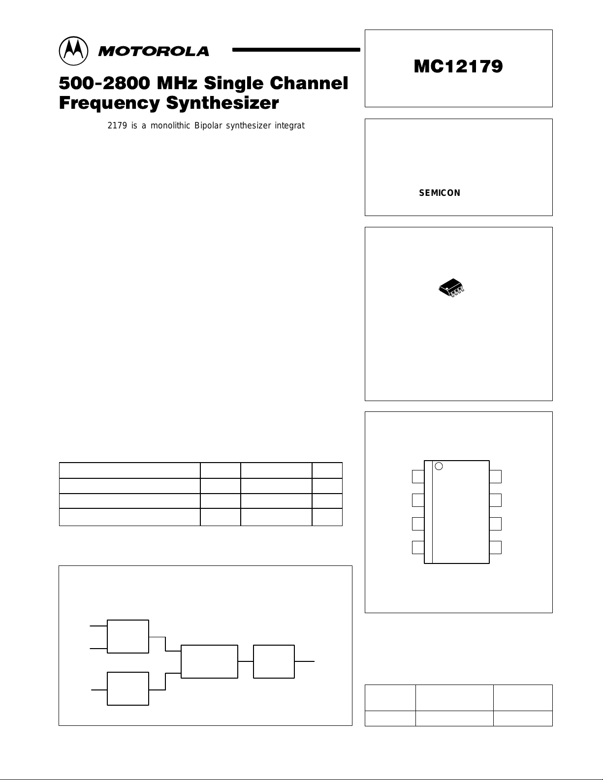
Block Diagram
OSC
OSC
out
F
in
in
Crystal
Oscillator
Prescaler
÷
256
f
r
Phase/Frequency
Detector
f
v
Charge
Pump
PD
out
OSC
V
Gnd
in
CC
in
(Top View)
OSC
81
out
V
72
P
PD
63
out
GndPF
54
ORDERING INFORMATION
Operating
Device
MC12179D TA = –40° to +85°C SO–8
Motorola, Inc. 1997 Rev 3
Temperature Range
Package
MC12179
ELECTRICAL CHARACTERISTICS (V
Characteristic
Supply Current for V
Supply Current for V
Operating Frequency fINmax
Operating Frequency Crystal Mode
Input Sensitivity F
Input Sensitivity External Oscillator OSC
Output Source Current
Output Sink Current
Output Leakage Current (PD
NOTES: 1.VCC and VP = 5.5 V; FIN = 2.56 GHz; F
2.AC coupling, FIN measured with a 1000 pF capacitor.
3.Assumes C1 and C2 (Figure 1) limited to ≤30 pF each including stray and parasitic capacitances.
4.AC coupling to OSCin.
5.Refer to Figure 15 and Figure 16 for typical performance curves over temperature and power supply voltage.
CC
P
External Oscillator OSC
5
5
= 4.5 to 5.5 V; VP = VCC to 5.5 V; TA = –40 to 85°C, unless otherwise noted.)
CC
Symbol Min Typ Max Unit Condition
fINmin
in
in
in
(PD
) I
out
(PD
) I
out
) I
out
= 10 MHz crystal; PD
OSC
I
F
F
OSC
V
V
OSC
CC
I
P
IN
IN
OH
OL
OZ
– 3.1 5.6 mA Note 1
– 0.4 1.3 mA Note 1
2800
–
5
2
200 – 1000 mV
500 – 2200 mV
–2.8 –2.2 –1.6 mA VP = 4.5 V, V
1.6 2.2 2.8 mA VP = 4.5 V, V
– 0.5 15 nA VP = 5.0 V, V
open.
out
–
–
–
–
–
500
11
11
MHz Note 2
MHz Note 3
P–P
P–P
Note 4
Note 2
Note 4
= VP/2
= VP/2
= VP/2
PIN FUNCTION DESCRIPTION
Pin Symbol I/O Function
1 OSCin I Oscillator Input — An external parallel–resonant, fundamental crystal is connected between OSC
2 V
3 Gnd — Ground.
4 F
5 GndP — Ground — For charge pump circuitry.
6 PD
7 V
8 OSCout O Oscillator output, for use with an external crystal as shown in Figure 1.
CC
in
out
P
and OSC
shown in Figure 1, are required to set the proper crystal load capacitance and oscillator frequency.
For an external reference oscillator, an external signal is AC–coupled to the OSCin pin with a
1000 pF coupling capacitor, with no connection to OSC
value of 50 kΩ MUST be placed across the OSCin and OSC
— Positive Power Supply. Bypass capacitors should be placed as close as possible to the pin and be
connected directly to the ground plane.
I
Prescaler Input — The VCO signal is AC coupled into the F
O Single ended phase/frequency detector output (charge pump output). Three–state current
sink/source output for use as a loop error signal when combined with an external low pass filter. The
phase/frequency detector is characterized by a linear transfer function.
— Positive power supply for charge pump. VP MUST be equal or greater than VCC. Bypass capacitors
should be placed as close as possible to the pin and be connected directly to the ground plane.
to form an internal reference oscillator (crystal mode). External capacitors C1 and C2, as
out
. In either mode, a resistor with a nominal
out
pins for proper operation.
out
pin.
in
PDout
PDout
PDout
in
2
MOTOROLA RF/IF DEVICE DATA
+5.0 V
2
C1
C2
NOTE: External 50 kΩ resistor
across Pins 1 and 8 is necessary in
either crystal or driven mode.
VCO
1
8
4
1000 pF
MC12179
Figure 1. MC12179 Expanded Block Diagram
V
CC
OSC
in
Crystal
in
Oscillator
out
Prescaler
÷
256
GND GNDP
f
r
Phase/Frequency
Detector
f
v
OSC
F
Charge
Pump
53
PD
V
out
+5.0 V
7
P
6
To Loop Filter
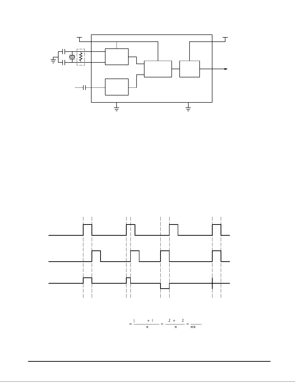
PHASE CHARACTERISTICS
The phase comparator in the MC12179 is a high speed
digital phase/frequency detector circuit. The circuit
determines the “lead” or “lag” phase relationship and time
difference between the leading edges of the VCO (fv) signal
and the reference (fr) input. The detector can cover a range of
±2π radian of fv/fr phase difference. The operation of the
charge pump output is shown in Figure 2.
fr lags fv in phase OR fv>fr in frequency
When the phase of fr lags that of fv or the frequency of fv is
greater than fr, the Do output will sink current. The pulse
width will be determined by the time difference between the
two rising edges.
Figure 2. Phase/Frequency Detector and Charge Pump Waveforms
f
r
(OSCin)
f
v
(Fin
÷
256)
fr leads fv in phase OR fv<fr in frequency
When the phase of fr leads that of fv or the frequency of f
is less than fr, the Do output will source current. The pulse
width will be determined by the time difference between the
two rising edges.
fr = fv in phase and frequency
When the phase and frequency of fr and fv are equal, the
charge pump will be in a quiet state, except for current spikes
when signals are in phase. This situation indicates that the
loop is in lock and the phase comparator will maintain the
loop in its locked state.
H
L
H
L
v
PD
out
Kp–Charge Pump Gain
MOTOROLA RF/IF DEVICE DATA
H = High voltage level; L = Low voltage level; Z = High impedance
NOTES: Phase difference detection range:
|I
|)|I
source
[
4
p
sink
∼ –2π
|
|2.2|)|–2.2|
+
to 2
4
p
π
1.1 mA
+
p
radian
Sourcing Current Pulse
Z
Sinking Current Pulse
3
MC12179
APPLICATIONS INFORMATION
The MC12179 is intended for applications where a fixed
local oscillator is required to be synthesized. The prescaler
on the MC12179 operates up to 2.8GHz which makes the
part ideal for many satellite receiver applications as well as
applications in the 2nd ISM (Industrial, Scientific, and
Medical) band which covers the frequency range of
2400MHz to 2483MHz. The part is also intended for MMDS
(Multi–channel Multi–point Distribution System) block
downconverter applications. Below is a typical block diagram
of the complete PLL.
Figure 3. T ypical Block Diagram of Complete PLL
External Ref
10.0 MHz
MC12179 PLL
φ
/Freq
Charge
Det
256
Pump
÷
P
Loop
Filter
VCO
2560.00 MHz
As can be seen from the block diagram, with the addition
of a VCO, a loop filter, and either an external oscillator or
crystal, a complete PLL sub–system can be realized. Since
most of the PLL function is integrated into the MC12179, the
user’s primary focus is on the loop filter design and the
crystal reference circuit. Figure 13 and Figure 14 illustrate
typical VCO spectrum and phase noise characteristics.
Figure 17 and Figure 18 illustrate the typical input impedance
versus frequency for the prescaler input.
Crystal Oscillator Design
The MC12179 is used as a multiply–by–256 PLL circuit
which transfers the high stability characteristic of a low
frequency reference source to the high frequency VCO in the
PLL loop. T o facilitate this, the device contains an input circuit
which can be configured as a crystal oscillator or a buffer for
accepting an external signal source.
In the external reference mode, the reference source is
AC–coupled into the OSCin input pin. The input level signal
should be between 500–2200 mVpp. When configured with
an external reference, the device can operate with input
frequencies down to 2MHz, thus allowing the circuit to control
the VCO down to 512 MHz. To optimize the phase noise of
the PLL when used in this mode, the input signal amplitude
should be closer to the upper specification limit. This
maximizes the slew rate of the input signal as it switches
against the internal voltage reference.
In the crystal mode, an external parallel–resonant
fundamental mode crystal is connected between the OSC
and OSC
pins. This crystal must be between 5.0 MHz and
out
11 MHz. External capacitors, C1 and C2 as shown in
Figure 1, are required to set the proper crystal load
capacitance and oscillator frequency. The values of the
capacitors are dependent on the crystal chosen and the input
capacitance of the device and any stray board capacitance.
In either mode, a 50kΩ resistor must be connected
between the OSCin and the OSC
pins for proper device
out
operation. The value of this resistor is not critical so a 47kΩ or
51kΩ ±10% resistor is acceptable.
Since the MC12179 is realized with an all–bipolar ECL
style design, the internal oscillator circuitry is different from
more traditional CMOS oscillator designs which realize the
crystal oscillator with a modified inverter topology. These
CMOS designs typically excite the crystal with a rail–to–rail
signal which may overdrive the crystal resulting in damage or
unstable operation. The MC12179 design does not exhibit
these phenomena because the swing out of the OSC
out
pin is
less than 600mV. This has the added advantage of
minimizing EMI and switching noise which can be generated
by rail–to–rail CMOS outputs. The OSC
output should not
out
be used to drive other circuitry.
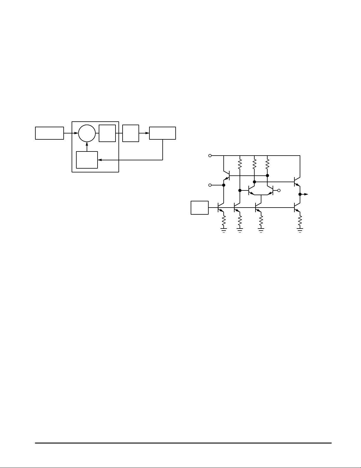
The oscillator buffer in the MC12179 is a single stage, high
speed, differential input/output amplifier; it may be
considered to be a form of the Pierce oscillator. A simplified
circuit diagram is seen in Figure 4.
Figure 4. Simplified Crystal Oscillator/Buffer Circuit
V
CC
OSC
out
Bias
Source
OSC
in
To Phase/
Frequency
Detector
OSCin drives the base of one input of an NPN transistor
differential pair . The non–inverting input of the differential pair
is internally biased. OSC
is the inverted input signal and is
out
buffered by an emitter follower with a 70 µA pull–down
current and has a voltage swing of about 600 mVpp. Open
loop output impedance is about 425Ω. The opposite side of
the differential amplifier output is used internally to drive
another buffer stage which drives the phase/frequency
detector. With the 50 kΩ feedback resistor in place, OSC
and OSC
are biased to approximately 1.1V below VCC.
out
in
The amplifier has a voltage gain of about 15 dB and a
bandwidth in excess of 150 MHz. Adherence to good RF
design and layout techniques, including power supply pin
decoupling, is strongly recommended.
A typical crystal oscillator application is shown in Figure 1.
The crystal and the feedback resistor are connected directly
between OSCin and OSC
, while the loading capacitors, C1
out
and C2, are connected between OSCin and ground, and
in
OSC
that as far as the crystal is concerned, the two loading
and ground respectively . It is important to understand
out
capacitors are in series (albeit through ground). So when the
crystal specification defines a specific loading capacitance,
this refers to the total external (to the crystal) capacitance
seen across its two pins.
This capacitance consists of the capacitance contributed
by the amplifier (IC and packaging), layout capacitance, and
the series combination of the two loading capacitors. This is
illustrated in the equation below:
4
MOTOROLA RF/IF DEVICE DATA

MC12179
CI+
C
AMP
)
C
STRAY
C1 C2
)
C1)C2
Provided the crystal and associated components are
located immediately next to the IC, thus minimizing the stray
capacitance, the combined value of C
AMP
and C
STRAY
is
approximately 5pF. Note that the location of the OSCin and
OSC
pins at the end of the package, facilitates placing the
out
crystal, resistor and the C1 and C2 capacitors very close to
the device. Usually , one of the capacitors is in parallel with an
adjustable capacitor used to trim the frequency of oscillation.
It is important that the total external (to the IC) capacitance
seen by either OSCin or OSC
, be no greater than 30pF.
out
In operation, the crystal oscillator will start up with the
application of power. If the crystal is in a can that is not
grounded it is often possible to monitor the frequency of
oscillation by connecting an oscilloscope probe to the can;
this technique minimizes any disturbance to the circuit. If a
malfunction is indicated, a high impedance, low capacitance,
FET probe may be connected to either OSCin or OSC
out
Signals typically seen at those points will be very nearly
sinusoidal with amplitudes of roughly 300 to 600 mVpp.
Some distortion is inevitable and has little bearing on the
accuracy of the signal going to the phase detector.
Loop Filter Design
Because the device is designed for a non–frequency agile
synthesizer (i.e., how fast it tunes is not critical) the loop filter
design is very straight forward. The current output of the
charge pump allows the loop filter to be realized without the
need of any active components. The preferred topology for
the filter is illustrated below in Figure 5.
Figure 5. Loop Filter
Xtl
Osc
MC12179
Ph/Frq
÷
Det
256
N
Chrg
Pump
K
p
R
R
o
C
o
x
C
a
VCO
K
v
C
x
The Ro/Co components realize the primary loop filter. Ca is
added to the loop filter to provide for reference sideband
suppression. If additional suppression is needed, the Rx/C
realizes an additional filter. In most applications, this will not
be necessary. If all components are used, this results in a 4th
order PLL, which makes analysis difficult. To simplify this, the
loop design will be treated as a 2nd order loop (Ro/Co) and
additional guidelines are provided to minimize the influence
of the other components. If more rigorous analysis is needed,
mathematical/system simulation tools can be used.
Component Guideline
C
a
R
x
C
x
<0.1 × C
>10 × R
<0.1 × C
o
o
o
The focus of the design effort is to determine what the
loop’s natural frequency , ωo, should be. This is determined by
Ro, Co, Kp, Kv, and N. Because Kp, Kv, and N are given, it is
only necessary to calculate values for Ro and Co. There are
3 considerations in selecting the loop bandwidth:
1) Maximum loop bandwidth for minimum tuning speed
2) Optimum loop bandwidth for best phase noise
performance
3) Minimum loop bandwidth for greatest reference
sideband suppression
Usually a compromise is struck between these 3 cases,
however, for the fixed frequency application, minimizing the
.
tuning speed is not a critical parameter.
To specify the loop bandwidth for optimal phase noise
performance, an understanding of the sources of phase
noise in the system and the effect of the loop filter on them is
required. There are 3 major sources of phase noise in the
phase–locked loop – the crystal reference, the VCO, and the
loop contribution. The loop filter acts as a low–pass filter to
the crystal reference and the loop contribution equal to the
total divide–by–N ratio. This is mathematically described in
Figure 10. The loop filter acts as a high–pass filter to the VCO
with an in–band gain equal to unity. This is described in
Figure 11. The loop contribution includes the PLL IC, as well
as noise in the system; supply noise, switching noise, etc.
For this example, a loop contribution of 15 dB has been
selected, which corresponds to data in Figure 14.
The crystal reference and the VCO are characterized as
high–order 1/f noise sources. Graphical analysis is used to
determine the optimum loop bandwidth. It is necessary to
have noise plots from the manufacturer. This method
provides a straightforward approximation suitable for quickly
estimating the optimal bandwidth. The loop contribution is
characterized as white–noise or low–order 1/f noise given in
the form of a noise factor which combines all the noise effects
into a single value. The phase noise of the Crystal Reference
is increased by the noise factor of the PLL IC and related
circuitry. It is further increased by the total divide–by–N ratio
x
of the loop. This is illustrated in Figure 6.
The point at which the VCO phase noise crosses the
amplified phase noise of the Crystal Reference is the point of
the optimum loop bandwidth. In the example of Figure 6, the
optimum bandwidth is approximately 15 KHz.
MOTOROLA RF/IF DEVICE DATA
5

MC12179
Figure 6. Graphical Analysis of Optimum Bandwidth
–60
–70
–80
–90
–100
dB
–110
–120
–130
–140
–150
Figure 7. Closed Loop Frequency Response for ζ = 1
dB
To simplify analysis further a damping factor of 1 will be
selected. The normalized closed loop response is illustrated
in Figure 7 where the loop bandwidth is 2.5 times the loop
natural frequency (the loop natural frequency is the
frequency at which the loop would oscillate if it were
unstable). Therefore the optimum loop bandwidth is
Crystal Reference
10 100 1k 10k 100k 1M
Hz
Natural Frequency
10
0
–10
–20
–30
–40
–50
–60
0.1 1k
1 10 100
3dB Bandwidth
Optimum Bandwidth
20*log(256)
15dB NF of the Noise
Contribution from Loop
Hz
VCO
15kHz/2.5 or 6kHz (37.7krads) with a damping coefficient,
ζ ≈ 1. T(s) is the transfer function of the loop filter.
Figure 8. Design Equations for the 2nd Order System
2
z
ǒ
Ǔ
s)1
w
o
2
s2)
Co[
Ro+
z
ǒ
Ǔ
s)1
w
o
KpK
v
ǒ
Ǔ
2
N
w
o
2
z
ǒ
Ǔ
woC
o
1
ǒ
Ǔ
2
w
o
³
³
T(s)
+
NC
o
ǒ
Ǔ
KpK
v
RoCo+
In summary, follow the steps given below:
Step 1: Plot the phase noise of crystal reference and the
VCO on the same graph.
Step 2: Increase the phase noise of the crystal reference by
the noise contribution of the loop.
Step 3: Convert the divide–by–N to dB (20log 256 – 48 dB)
and increase the phase noise of the crystal
reference by that amount.
Step 4: The point at which the VCO phase noise crosses the
amplified phase noise of the Crystal Reference is the
point of the optimum loop bandwidth. This is
approximately 15 kHz in Figure 6.
Step 5: Correlate this loop bandwidth to the loop natural
frequency and select components per Figure 8. In
this case the 3.0 dB bandwidth for a damping
coefficient of 1 is 2.5 times the loop’s natural
frequency . The relationship between the 3.0 dB loop
bandwidth and the loop’s “natural” frequency will
vary for different values of ζ. Making use of the
equations defined above in a math tool or spread
sheet is useful. To aid in the use of such a tool the
equations are summarized in Figures 9 through 11.
ǒ
+
RoCos)1
NC
o
Ǔ
s2)
KpK
v
1
ǒ
2
w
o
2
z
ǒ
w
o
Ǔ
³
Ǔ
³z+
RoCos)1
KpK
Ǹ
wo+
woRoC
ǒ
2
NC
+
v
o
o
Ǔ
Figure 9. Loop Parameter Relations
NC
o
Let:
KpK
Let: Ca+
Let: RoCo+
Let: K3w3+
6
1
+
2
w
v
o
aCo,Cx+
1
,RxCx+
w
3
wo,K4w4+
,RoCo+
2
z
w
o
bCo,A+1)a , and B+1)a)b
1
,Ro(Ca)
w
4
wo,K5w5+
w
Cx)
o
1
+
w
5
MOTOROLA RF/IF DEVICE DATA

MC12179
Figure 10. Transfer Function for the Crystal Noise in the Frequency Plane
w
ǒ
Ǔ
2
T(jw)+N
@
ǒ
1)K3K
4
w
4
4
w
o
*
2
w
B
2
w
o
Figure 11. Transfer Function for the VCO Noise in the Frequency Plane
1)j
z
w
o
3
jǒ2
w
z
*
(AK4)
w
o
Ǔ
)
K5)
w
Ǔ
3
w
o
4
K3K
w
*
4
4
w
o
4
w
*
4
B
4
w
o
T(jw)
+
ǒ
1)K3K
ǒ
Appendix: Derivation of Loop Filter Transfer Function
The purpose of the loop filter is to convert the current from
the phase detector to a tuning voltage for the VCO. The total
transfer function is derived in two steps. Step 1 is to find the
voltage generated by the impedance of the loop filter. Step 2
is to find the transfer function from the input of the loop filter to
its output. The “voltage” times the “transfer function” is the
Figure 12. Overall Transfer Function of the PLL
For the 2nd Order PLL:
V
p
R
o
C
o
V
t
ZLF(s)
TLF(s)
+
+
2
w
Ǔ
B
*
2
w
o
2
w
Ǔ
)
jǒ2
2
w
o
overall transfer function of the loop filter. To use these
equations in determining the overall transfer function of a PLL
multiply the filter’s impedance by the gain constant of the
phase detector then multiply that by the filter’s transfer
function (which is unity in the 2nd and 3rd order cases
below).
RoCos)1
Cos
Vt(s)
+
Vp(s)
1,Vp(s)+Kp(s)ZLF(s)
jǒ(AK4)
w
z
*
w
o
K5)
(AK4)
3
w
Ǔ
3
w
o
3
w
Ǔ
K5)
3
w
o
For the 3rd Order PLL:
For the 4th Order PLL:
V
p
V
p
ZLF(s)
TLF(s)
MOTOROLA RF/IF DEVICE DATA
V
t
R
C
C
o
o
a
ZLF(s)
+
RoCos)1
CoRoCas2)
(Co)
Ca)s
Vt(s)
TLF(s)
+
R
R
o
C
o
x
C
a
C
x
Vp(s)
V
+
1,Vp(s)+Kp(s)ZLF(s)
t
(RoCos)1) (RxCxs)1)
+
CoRoCaRxCxs3)[(Co)
+
Vt(s)
Vp(s)
+
1
(RxCxs)1)
Ca)RxCx)
CoRo(Cx)
,Vp(s)+Kp(s)ZLF(s)
Ca)]s2)
(Co)
Ca)
Cx)s
7

MC12179
Figure 13. VCO Output Spectrum with MC12179, VCC = 5.0 V
(ECLiPTEK 8.9 MHz Crystal and ZCOM 2500 VCO)
NOTE: Spurs can be reduced further by narrowing the loop bandwidth of the PLL loop filter and/or
adding an extra filter (Rx/Cx)
Figure 14. T ypical Phase Noise Plot, 2200 MHz VCO
(With the MC12179 in a Closed Loop)
HP 3048A CARRIER 2200MHz
0
–25
–50
–75
dBc/Hz
–100
–125
–150
–170
1k 10k 100k 1M 10M 40M
L
(f) [dBc/Hz] vs f[Hz]
8
MOTOROLA RF/IF DEVICE DATA

MC12179
Figure 15. T ypical Charge Pump Current versus Temperature
(VCC = Vpp = 5.0 V)
2.5
2.0
1.5
1.0
0.5
0.0
–0.5
Sink/Source Current (mA)
–1.0
–1.5
–2.0
–2.5
0 0.5 1.0 1.5 2.0 2.5 3.0 3.5 4.0 4.5 5.0
SINK
SOURCE
Voltage at PD
out
(V)
–40°C
+25
°
+85
°
C
C
Figure 16. T ypical Charge Pump Current versus Voltage
(T = 25°C)
2.5
2.0
SINK
1.5
1.0
0.5
0.0
–0.5
Sink/Source Current (mA)
–1.0
–1.5
–2.0
–2.5
SOURCE
0 0.5 1.0 1.5 2.0 2.5 3.0 3.5 4.0 4.5 5.0 5.5
Voltage at PD
out
(V)
4.5V VCC/V
5.0V V
5.5V VCC/V
PP
CC/VPP
PP
MOTOROLA RF/IF DEVICE DATA
9

MC12179
Figure 17. T ypical Real Input Impedance versus Input Frequency
(For the Fin Input)
100
80
60
R (Ohms)
40
20
0
250 500 750 1000 1250 1500 1750 2000 2250 2500 2750
Frequency (MHz)
Figure 18. T ypical Imaginary Input Impedance versus Input Frequency
(For the Fin Input)
50
25
0
–25
–50
–75
–100
jX (Ohms)
–125
–150
–175
–200
–225
–250
250 500 750 1000 1250 1500 1750 2000 2250 2500 2750
Frequency (MHz)
10
MOTOROLA RF/IF DEVICE DATA

C
A
E
B
A1
MC12179
OUTLINE DIMENSIONS
D SUFFIX
PLASTIC PACKAGE
CASE 751-06
(SO–8)
ISSUE T
D
58
0.25MB
1
H
4
e
M
h
X 45
_
q
C
A
SEATING
PLANE
0.10
L
B
SS
A0.25MCB
NOTES:
1. DIMENSIONING AND TOLERANCING PER ASME
Y14.5M, 1994.
2. DIMENSIONS ARE IN MILLIMETER.
3. DIMENSION D AND E DO NOT INCLUDE MOLD
PROTRUSION.
4. MAXIMUM MOLD PROTRUSION 0.15 PER SIDE.
5. DIMENSION B DOES NOT INCLUDE DAMBAR
PROTRUSION. ALLOWABLE DAMBAR
PROTRUSION SHALL BE 0.127 TOTAL IN EXCESS
OF THE B DIMENSION AT MAXIMUM MATERIAL
CONDITION.
MILLIMETERS
DIM MIN MAX
A 1.35 1.75
A1 0.10 0.25
B 0.35 0.49
C 0.19 0.25
D 4.80 5.00
E
3.80 4.00
1.27 BSCe
H 5.80 6.20
h
0.25 0.50
L 0.40 1.25
0 7
q
__
Motorola reserves the right to make changes without further notice to any products herein. Motorola makes no warranty , representation or guarantee regarding
the suitability of its products for any particular purpose, nor does Motorola assume any liability arising out of the application or use of any product or circuit, and
specifically disclaims any and all liability, including without limitation consequential or incidental damages. “T ypical” parameters which may be provided in Motorola
data sheets and/or specifications can and do vary in different applications and actual performance may vary over time. All operating parameters, including “Typicals”
must be validated for each customer application by customer’s technical experts. Motorola does not convey any license under its patent rights nor the rights of
others. Motorola products are not designed, intended, or authorized for use as components in systems intended for surgical implant into the body, or other
applications intended to support or sustain life, or for any other application in which the failure of the Motorola product could create a situation where personal injury
or death may occur. Should Buyer purchase or use Motorola products for any such unintended or unauthorized application, Buyer shall indemnify and hold Motorola
and its officers, employees, subsidiaries, affiliates, and distributors harmless against all claims, costs, damages, and expenses, and reasonable attorney fees
arising out of, directly or indirectly, any claim of personal injury or death associated with such unintended or unauthorized use, even if such claim alleges that
Motorola was negligent regarding the design or manufacture of the part. Motorola and are registered trademarks of Motorola, Inc. Motorola, Inc. is an Equal
Opportunity/Affirmative Action Employer.
How to reach us:
USA/EUROPE/Locations Not Listed: Motorola Literature Distribution; JAPAN: Nippon Motorola Ltd.: SPD, Strategic Planning Office, 141,
P.O. Box 5405, Denver, Colorado 80217. 1–303–675–2140 or 1–800–441–2447 4–32–1 Nishi–Gotanda, Shagawa–ku, Tokyo, Japan. 03–5487–8488
Customer Focus Center: 1–800–521–6274
Mfax: RMFAX0@email.sps.mot.com – TOUCHTONE 1–602–244–6609 ASIA/PACIFIC: Motorola Semiconductors H.K. Ltd.; 8B Tai Ping Industrial Park,
Moto rola Fax Back Sys tem – US & Canada ONLY 1–800–774–1848 51 Ting Kok Road, Tai Po, N.T., Hong Kong. 852–26629298
HOME PAGE: http://motorola.com/sps/
MOTOROLA RF/IF DEVICE DATA
– http://sps.motorola.com/mfax/
◊
Mfax is a trademark of Motorola, Inc.
MC12179/D
11
 Loading...