

SEMICONDUCTOR
TECHNICAL DATA
LOW POWER
VOLTAGE CONTROLLED
OSCILLATOR
Order this document by MC12148/D
8
1
GND
V
CC
7
2
VCCO
AGC
6
3
Out
TANK
5
4
GND
V
ref
Device
Operating
Temperature Range
Package
ORDERING INFORMATION
MC12148D
MC12148SD
TA = – 40° to +85°C
SO–8
SSOP–8
D SUFFIX
PLASTIC PACKAGE
CASE 751
(SO–8)
8
1
(Top View)
PIN CONNECTIONS
SD SUFFIX
PLASTIC PACKAGE
CASE 940
(SSOP–8)
8
1
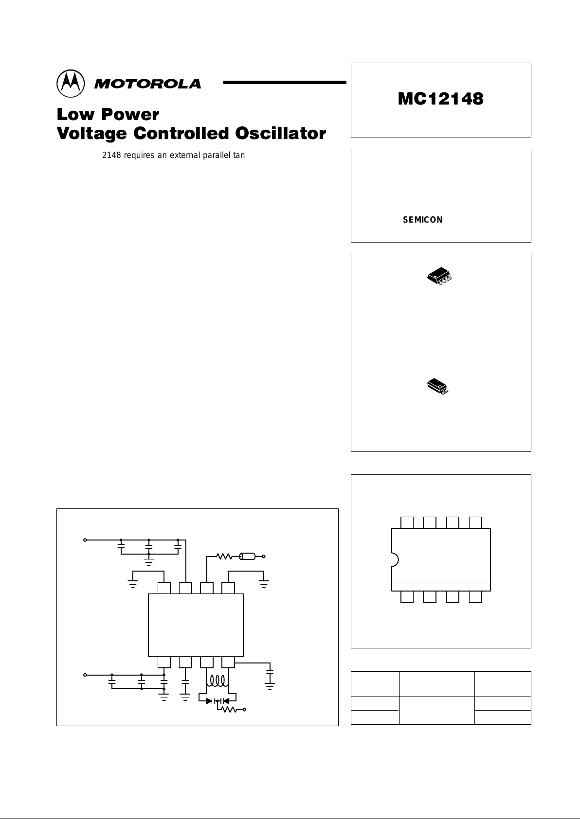
The MC12148 requires an external parallel tank circuit consisting of the
inductor (L) and capacitor (C). A varactor diode may be incorporated into the
tank circuit to provide a voltage variable input for the oscillator (VCO). This
device may also be used in many other applications requiring a fixed
frequency clock.
The MC12148 is ideal in applications requiring a local oscillator. Systems
include electronic test equipment and digital high–speed
telecommunications.
The MC12148 is based on the VCO circuit topology of the MC1648. The
MC12148 has been realized utilizing Motorola’s MOSAIC III advanced
bipolar process technology which results in a design which can operate at a
much higher frequency than the MC1648 while utilizing half the current.
Please consult with the MC1648 data sheet for additional background
information.
The ECL output circuitry of the MC12148 is not a traditional open emitter
output structure and instead has an on–chip termination resistor with a
nominal value of 500 ohms. This facilitates direct ac–coupling of the output
signal into a transmission line. Because of this output configuration, an
external pull–down resistor is not required to provide the output with a dc
current path. This output is intended to drive one ECL load. If the user
needs to fanout the signal, an ECL buffer such as the MC10EL16 Line
Receiver/Driver should be used.
NOTE: The MC12148 is NOT useable as a crystal oscillator.
• Typical Operating Frequency Up to 1100 MHz
• Low–Power 20 mA at 5.0 Vdc Power Supply
• 8–Pin SOIC Package
• Phase Noise –90 dBc/Hz at 25 kHz Typical
Motorola, Inc. 1997 Rev 5
BLOCK DIAGRAM
(Typical Test Circuit)
7865
2134
GND VCCO Out GND
VCCAGC TANK V
ref
1200Ω*
F
out
V
in
51K
Ω
0.1µF
* The 1200
Ω
resistor
and the scope
termination impedance
constitute a 25:1
attenuator probe.
0.1µF0.01µF 100µF
0.1
µ
F
100
µ
F
0.01µF
0.1µF
VCCO
VCC = 4.5 to 5.5 V
MC12148
2
MOTOROLA RF/IF DEVICE DATA
MAXIMUM RATINGS
Parameter
Symbol Value Unit
Power Supply Voltage, Pins 1, 7 V
CC
–0.5 to 7.0 Vdc
Operating Temperature Range T
A
–40 to 85 °C
Storage Temperature Range T
stg
–65 to 150 °C
NOTE: ESD data available upon request.
ELECTRICAL CHARACTERISTICS (V
CC
= 5.0 V; TA = –40 to 85°C, unless otherwise noted.)
Characteristic
Symbol Min Typ Max Unit
Supply Current I
CC
– 19 25 mA
Output Level HIGH (1.0 MΩ Impedance) V
OH
3.95 4.17 4.61 V
Output Level LOW (1.0 MΩ Impedance) V
OL
3.04 3.41 3.60 V
CSR @ 25 kHz Offset, 1.0 Hz BW
L
(f)
– –90 – dBc/Hz
CSR @ 1.0 MHz Offset, 1.0 Hz BW
L
(f)
– –120 – dBc/Hz
SNR (Signal to Noise Ratio from Carrier) SNR – 40 – dB
Frequency Stability Supply Drift Fsts – 3.6 – KHz/mV
Thermal Drift Fstt – 0.1 – KHz/°C
Second Harmonic (from Carrier) H2 – –25 – dBc
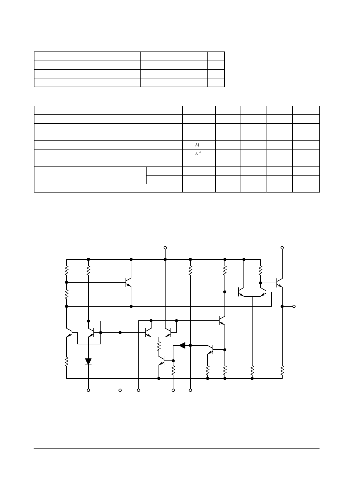
Figure 1. Circuit Schematic
2
AGC
5
GND
3
TANK
4
V
ref
8
GND
V
CC
1
V
CCO
7
Q4
Q3 Q2
Q1
Q5
D1
Q8
Q7 Q6
Q9
Q10Q11
D2
6
OUT
510
Ω
MC12148
3
MOTOROLA RF/IF DEVICE DATA
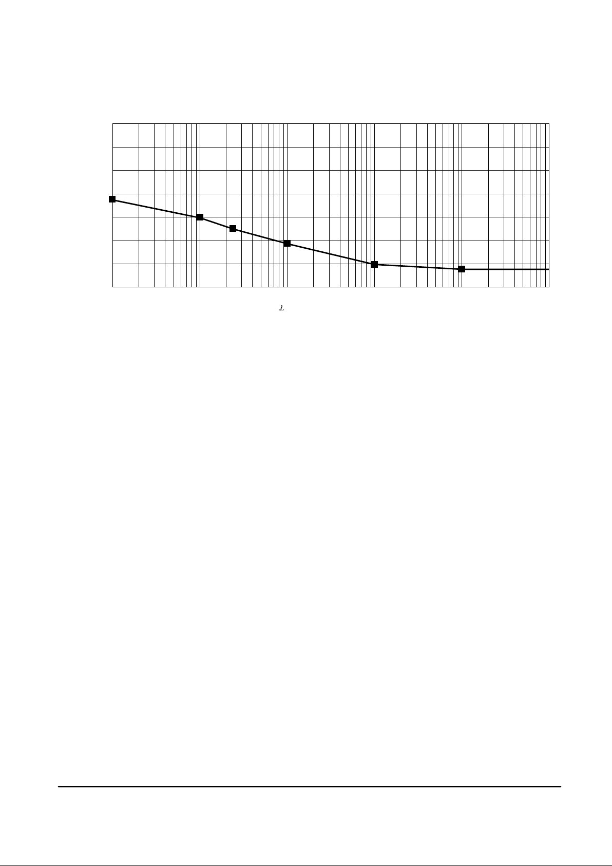
L
(f) [dBc/Hz] versus f [Hz]
Figure 2. Typical Evaluation Results
(CSR MC12148 5.0 Vdc; VCC @ 25°C; 930 MHz CW)
1K
–140
dBc/Hz
10K 100K 1M 10M 100M
–120
–100
–80
–60
–40
–20
0
Tank Component Suppliers
Below are suppliers who manufacture tuning varactors and inductors which can be used to build an external tank circuit.
Motorola has used these varactors and inductors for evaluation purposes, however, there are other vendors who manufacture
similar products.
Coilcraft Inductors A01T thru A05T
Coilcraft–Coilcraft, Inc.
1102 Silver Lake Rd.
Gary, Illinois 60013
708–639–6400
Loral Tuning Varactors GC1500 Series
Loral
16 Maple Road
Chelmsford, Massachusetts 01824
508–256–8101 or 508–256–4113
Alpha Tuning Diodes DVH6730 Series
Alpha Semiconductor Devices Division
20 Sylvan Road
Woburn, MA 01801
617–935–5150
* At 1.1 GHz, use a Coilcraft A0IT Springair coil at 2.5 nH and a Loral Varactor 3.0 to 8.0 pF at VIN = 1.0 to 5.0 V.

MC12148
4
MOTOROLA RF/IF DEVICE DATA
SD SUFFIX
PLASTIC PACKAGE
CASE 940-03
(SSOP–8)
ISSUE B
DIMAMIN MAX MIN MAX
INCHES
2.87 3.13 0.113 0.123
MILLIMETERS
B 5.20 5.38 0.205 0.212
C 1.73 1.99 0.068 0.078
D 0.05 0.21 0.002 0.008
F 0.63 0.95 0.024 0.037
G 0.65 BSC 0.026 BSC
H 0.44 0.60 0.017 0.023
J 0.09 0.20 0.003 0.008
J1 0.09 0.16 0.003 0.006
K 0.25 0.38 0.010 0.015
K1 0.25 0.33 0.010 0.013
____
NOTES:
1 DIMENSIONING AND TOLERANCING PER ANSI
Y14.5M, 1982.
2 CONTROLLING DIMENSION: MILLIMETER.
3 DIMENSION A DOES NOT INCLUDE MOLD FLASH,
PROTRUSIONS OR GATE BURRS. MOLD FLASH
OR GATE BURRS SHALL NOT EXCEED 0.15
(0.006) PER SIDE.
4 DIMENSION B DOES NOT INCLUDE INTERLEAD
FLASH OR PROTRUSION. INTERLEAD FLASH OR
PROTRUSION SHALL NOT EXCEED 0.15 (0.006)
PER SIDE.
5 DIMENSION K DOES NOT INCLUDE DAMBAR
PROTRUSION/INTRUSION. ALLOWABLE DAMBAR
PROTRUSION SHALL BE 0.13 (0.005) TOTAL IN
EXCESS OF K DIMENSION AT MAXIMUM
MATERIAL CONDITION. DAMBAR INTRUSION
SHALL NOT REDUCE DIMENSION K BY MORE
THAN 0.07 (0.002) AT LEAST MATERIAL
CONDITION.
6 TERMINAL NUMBERS ARE SHOWN FOR
REFERENCE ONLY.
7 DIMENSION A AND B ARE TO BE DETERMINED
AT DATUM PLANE –W–.
H
A
B
85
41
F
M
K8X REF
S
U
M
0.12 (0.005) V
S
T
L
L/2
PIN 1
IDENT
S
U
M
0.20 (0.008) T
–V–
–U–
D
C
0.076 (0.003)
G
–T–
SEATING
PLANE
DETAIL E
DETAIL E
–W–
N
N
0.25 (0.010)
K
J
J1
K1
SECTION N–N
L 7.65 7.90 0.301 0.311
M 0 8 0 8
D SUFFIX
PLASTIC PACKAGE
CASE 751–06
(SO–8)
ISSUE T
SEATING
PLANE
1
4
58
A0.25MCB
SS
0.25MB
M
h
q
C
X 45
_
L
DIM MIN MAX
MILLIMETERS
A 1.35 1.75
A1 0.10 0.25
B 0.35 0.49
C 0.19 0.25
D 4.80 5.00
E
1.27 BSCe
3.80 4.00
H 5.80 6.20
h
0 7
L 0.40 1.25
q
0.25 0.50
__
NOTES:
1. DIMENSIONING AND TOLERANCING PER ASME
Y14.5M, 1994.
2. DIMENSIONS ARE IN MILLIMETER.
3. DIMENSION D AND E DO NOT INCLUDE MOLD
PROTRUSION.
4. MAXIMUM MOLD PROTRUSION 0.15 PER SIDE.
5. DIMENSION B DOES NOT INCLUDE DAMBAR
PROTRUSION. ALLOWABLE DAMBAR
PROTRUSION SHALL BE 0.127 TOTAL IN EXCESS
OF THE B DIMENSION AT MAXIMUM MATERIAL
CONDITION.
D
E
H
A
B
e
B
A1
C
A
0.10
OUTLINE DIMENSIONS

MC12148
5
MOTOROLA RF/IF DEVICE DATA
Motorola reserves the right to make changes without further notice to any products herein. Motorola makes no warranty , representation or guarantee regarding
the suitability of its products for any particular purpose, nor does Motorola assume any liability arising out of the application or use of any product or circuit, and
specifically disclaims any and all liability, including without limitation consequential or incidental damages. “T ypical” parameters which may be provided in Motorola
data sheets and/or specifications can and do vary in different applications and actual performance may vary over time. All operating parameters, including “Typicals”
must be validated for each customer application by customer’s technical experts. Motorola does not convey any license under its patent rights nor the rights of
others. Motorola products are not designed, intended, or authorized for use as components in systems intended for surgical implant into the body, or other
applications intended to support or sustain life, or for any other application in which the failure of the Motorola product could create a situation where personal injury
or death may occur. Should Buyer purchase or use Motorola products for any such unintended or unauthorized application, Buyer shall indemnify and hold Motorola
and its officers, employees, subsidiaries, affiliates, and distributors harmless against all claims, costs, damages, and expenses, and reasonable attorney fees
arising out of, directly or indirectly, any claim of personal injury or death associated with such unintended or unauthorized use, even if such claim alleges that
Motorola was negligent regarding the design or manufacture of the part. Motorola and are registered trademarks of Motorola, Inc. Motorola, Inc. is an Equal
Opportunity/Affirmative Action Employer.
Mfax is a trademark of Motorola, Inc.
How to reach us:
USA/EUROPE/Locations Not Listed: Motorola Literature Distribution; JAPAN: Nippon Motorola Ltd.: SPD, Strategic Planning Office, 141,
P.O. Box 5405, Denver, Colorado 80217. 1–303–675–2140 or 1–800–441–2447 4–32–1 Nishi–Gotanda, Shagawa–ku, T o kyo, Japan. 03–5487–8488
Customer Focus Center: 1–800–521–6274
Mfax: RMFAX0@email.sps.mot.com – TOUCHTONE 1–602–244–6609 ASIA/PACIFIC: Motorola Semiconductors H.K. Ltd.; 8B Tai Ping Industrial Park,
Moto rola Fax Back System – US & Canada ONLY 1–800–774–1848 51 Ting Kok Road, Tai Po, N.T., Hong Kong. 852–26629298
– http://sps.motorola.com/mfax/
HOME PAGE: http://motorola.com/sps/
MC12148/D
◊
 Loading...