

Motorola MC12147SD, MC12147D Datasheet
8
1
NC
V
CC
7
2
Q
CNTL
6
3
GND
TANK
5
4
QB
V
REF
Device
Operating
Temperature Range
Package
SEMICONDUCTOR
TECHNICAL DATA
LOW POWER
VOLTAGE CONTROLLED
OSCILLATOR BUFFER
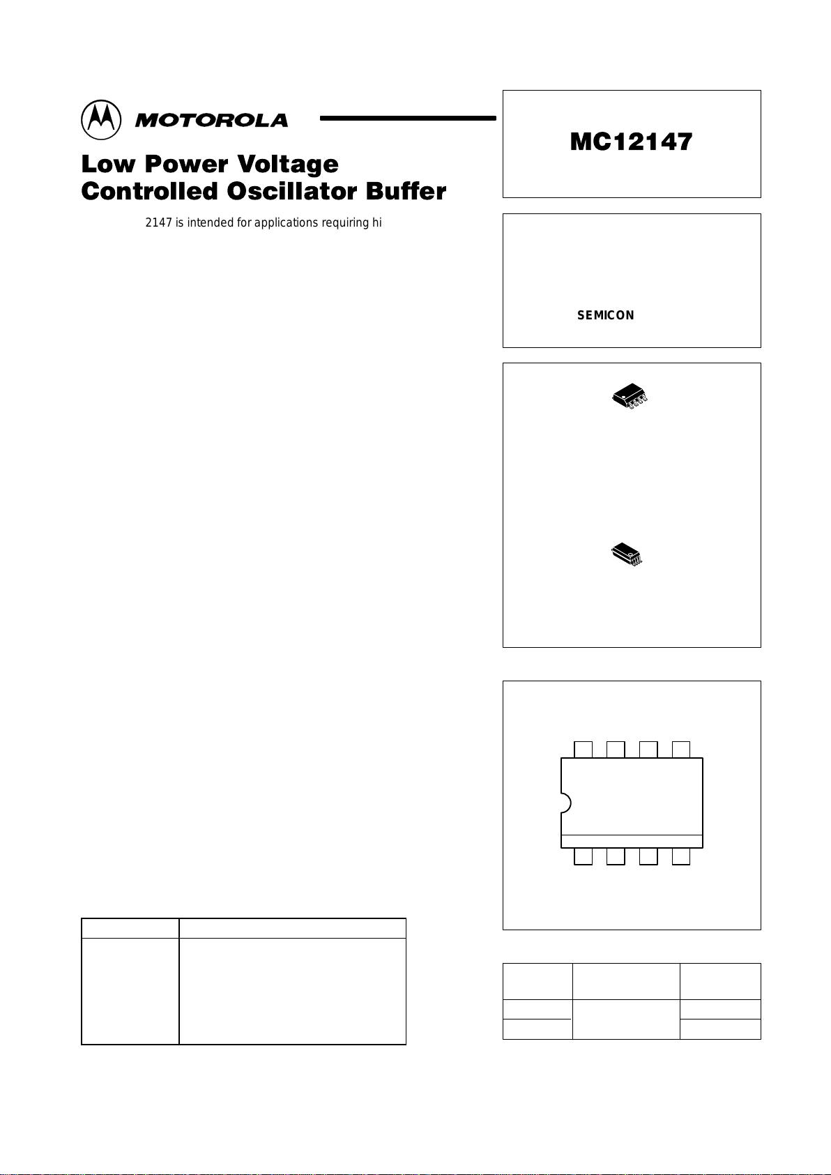
ORDERING INFORMATION
MC12147D
MC12147SD
TA = – 40° to +85°C
SO–8
SSOP–8
D SUFFIX
PLASTIC PACKAGE
CASE 751
(SO–8)
8
1
(Top View)
PIN CONNECTIONS
Order this document by MC12147/D
SD SUFFIX
PLASTIC PACKAGE
CASE 940
(SSOP–8)
8
1
The MC12147 is intended for applications requiring high frequency signal
generation up to 1300 MHz. An external tank circuit is used to determine the
desired frequency of operation. The VCO is realized using an
emitter–coupled pair topology . The MC12147 can be used with an integrated
PLL IC such as the MC12202 1.1 GHz Frequency Synthesizer to realize a
complete PLL sub–system. The device is specified to operate over a voltage
supply range of 2.7 to 5.5 V . It has a typical current consumption of 13 mA at
3.0 V which makes it attractive for battery operated handheld systems.
NOTE: The MC12147 is NOT suitable as a crystal oscillator.
• Operates Up to 1.3 GHz
• Space–Efficient 8–Pin SOIC or SSOP Package
• Low Power 13 mA Typical @ 3.0 V Operation
• Supply Voltage of 2.7 to 5.5 V
• Typical 900MHz Performance
– Phase Noise –105 dBc/Hz @ 100 kHz Offset
– Tuning Voltage Sensitivity of 20 MHz/V
• Output Amplitude Adjustment Capability
• Two High Drive Outputs With a Typical Range from –8.0 to –2.0 dBm
The device has two high frequency outputs which make it attractive for
transceiver applications which require both a transmit and receive local
oscillator (LO) signal. The outputs Q and QB are available for servicing the
receiver IF and transmitter up–converter single–ended. In receiver
applications, the outputs can be used together if it is necessary to generate a
differential signal for the receiver IF . Because the Q and QB outputs are open
collector, terminations to the VCC supply are required for proper operation.
Since the outputs are complementary, BOTH outputs must be terminated
even if only one is needed. The Q and QB outputs have a nominal drive level
of –8dBm to conserve power. If addition signal amplitude is needed, a level
adjustment pin (CNTL) is available, which when tied to ground, boosts the
nominal output levels to –2.0 dBm.
External components required for the MC12147 are: (1) tank circuit (LC
network); (2) Inductor/capacitor to provide the termination for the open
collector outputs; and (3) adequate supply voltage bypassing. The tank
circuit consists of a high–Q inductor and varactor components. The
preferred tank configuration allows the user to tune the VCO across the full
supply range. VCO performance such as center frequency, tuning voltage
sensitivity, and noise characteristics are dependent on the particular
components and configuration of the VCO tank circuit.
PIN NAMES
Pin Function
V
CC
CNTL
TANK
V
REF
QB
GND
Q
Power Supply
Amplitude Control for Q, QB Output Pair
Tank Circuit Input
Bias Voltage Output
Open Collector Output
Ground
Open Collector Output
Motorola, Inc. 1997 Rev 2
MC12147
2
MOTOROLA RF/IF DEVICE DATA
MAXIMUM RATINGS (Note 1)
Parameter
Symbol Value Unit
Power Supply Voltage, Pin 1 V
CC
-0.5 to +7.0 V
Operating Temperature Range T
A
–40 to +85 °C
Storage Temperature Range T
STG
-65 to +150 °C
Maximum Output Current, Pin 5,7 I
O
12 mA
NOTES: 1. Maximum Ratings are those values beyond which damage to the device may occur.
Functional operation should be restricted to the Recommended Operating Conditions.
2.ESD data available upon request.
ELECTRICAL CHARACTERISTICS (V
CC
= 2.7 to 5.5 VDC, TA = -40 to 85°C, unless otherwise noted.)
Characteristic
Symbol Min Typ Max Unit
Supply Current (CNTL=GND)VCC = 3.3 V
VCC = 5.5 V
I
CC
–
–
14.0
23.5
18
28
mA
Supply Current (CNTL=OPEN)VCC = 3.3 V
VCC = 5.5 V
I
CC
–
–
8
13
13.0
22.5
mA
Output Amplitude (Pin 5 & 7) {Note 1]
VCC = 2.7 V
50Ω to V
CC
VCC = 2.7 V
VOH,
V
OL
2.6
2.1
2.7
2.3
–
2.4
V
Output Amplitude (Pin 5 & 7)
[Note 1]
VCC = 5.5 V
50Ω to V
CC
VCC = 5.5 V
VOH,
V
OL
5.4
4.8
5.5
5.0
–
5.1
V
Tuning V oltage Sensitivity
[Notes 2 and 3]
T
stg
– 20 – MHz/V
Frequency of Operation F
C
100 – 1300 MHz
CSR at 10 kHz Offset, 1.0 Hz BW [Notes 2 and 3]
L
(f)
– –85 – dBc/Hz
CSR at 100 kHz Offset, 1.0 Hz BW [Notes 2 and 3]
L
(f)
– –105 – dBc/Hz
Frequency Stability [Notes 2 and 3]
Supply Drift
Thermal Drift
F
sts
f
stt
–
–
0.8
50
–
–
MHz/V
KHz/°C
NOTES: 1. CNTL pin tied to ground.
2.Actual performance depends on tank components selected.
3.See Figure 12, 750 MHz tank.
4.T = 25°C, VCC = 5.0 V ±10%
MC12147
3
MOTOROLA RF/IF DEVICE DATA
OPERA TIONAL CHARACTERISTICS
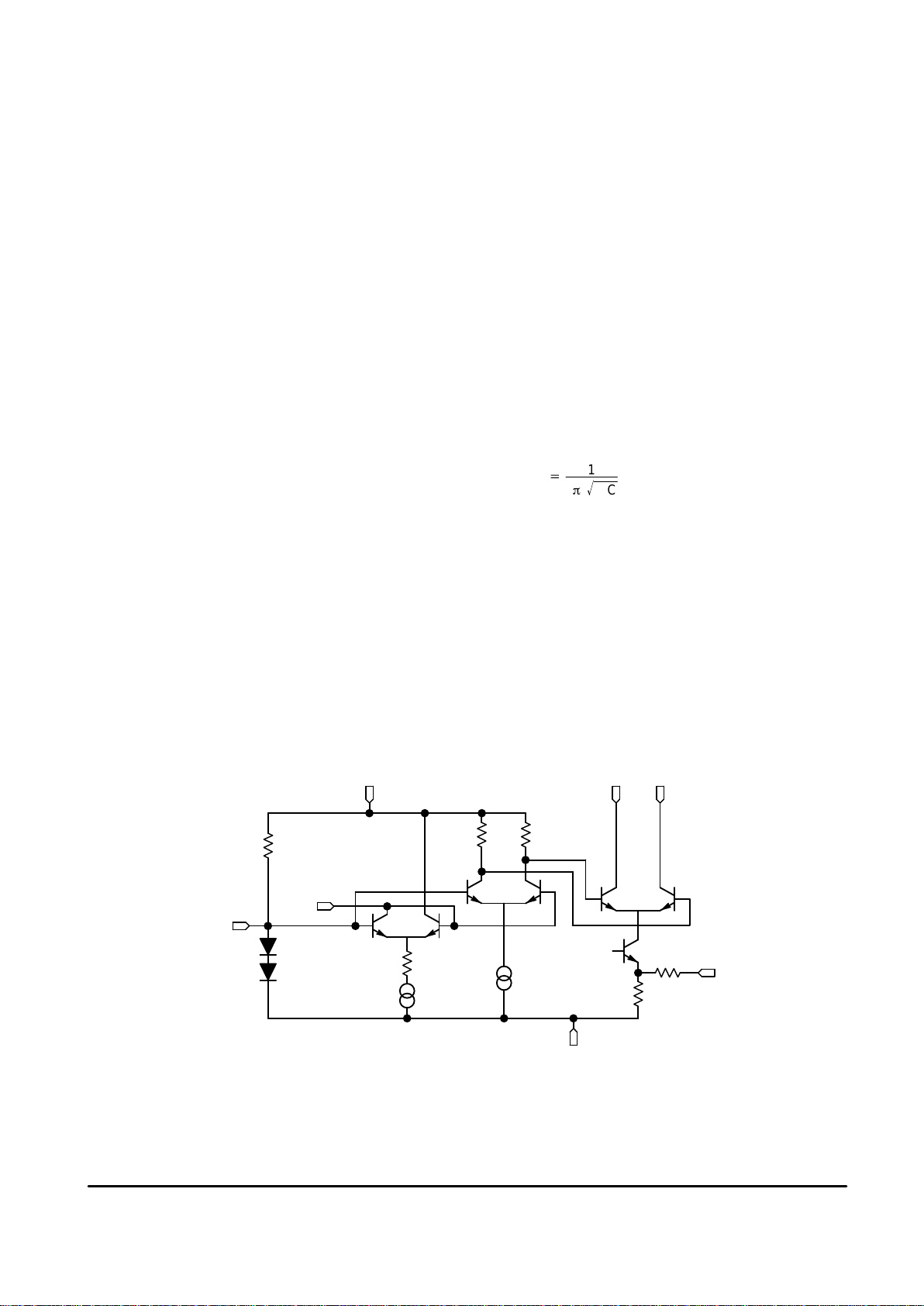
A simplified schematic of the MC12147 is found in
Figure 1. The oscillator incorporates positive feedback by
coupling the base of transistor Q2 to the collector of transistor
Q1. In order to minimize interaction between the VCO
outputs and the oscillator tank transistor pair, a buffer is
incorporated into the circuit. This differential buffer is realized
by the Q3 and Q4 transistor pair. The differential buffer drives
the gate which contains the primary open collector outputs, Q
and QB. The output is actually a current which has been set
by an internal bias driver to a nominal current of 4mA.
Additional circuitry is incorporated into the tail of the current
source which allows the current source to be increased to
approximately 10mA. This is accommodated by the addition
of a resistor which is brought out to the CNTL pin. When this
pin is tied to ground, the additional current is sourced through
the current source thus increasing the output amplitude of the
Q/QB output pair. If less than 10 mA of current is needed, a
resistor can be added to ground which reduces the amount of
current.
APPLICATION INFORMATION
Figure 2 illustrates the external components necessary for
the proper operation of the VCO buffer. The tank circuit
configuration in this figure allows the VCO to be tuned across
the full operating voltage of the power supply. This is very
important in 3V applications where it is desirable to utilize as
much of the operating supply range as possible so as to
minimize the VCO sensitivity (MHz/V). In most situations, it is
desirable to keep the sensitivity low so the circuit will be less
susceptible to external noise influences. An additional benefit
to this configuration is that additional regulation/ filtering can
be incorporated into the VCC line without compromising the
tuning range of the VCO. With the AC–coupled tank
configuration, the V
tune
voltage can be greater than the V
CC
voltage supplied to the device.
There are four main areas that the user directly influences
the performance of the VCO. These include Tank Design,
Output Termination Selection, Power Supply Decoupling,
and Circuit Board Layout/Grounding.
The design of the tank circuit is critical to the proper
operation of the VCO. This tank circuit directly impacts the
main VCO operating characteristics:
1) Frequency of Operation
2) Tuning Sensitivity
3) Voltage Supply Pushing
4) Phase Noise Performance
The tank circuit, in its simplest form, is realized as an LC
circuit which determines the VCO operating frequency. This
is described in Equation 1.
Equation 1
fo+
1
2pLC
Ǹ
In the practical case, the capacitor is replaced with a
varactor diode whose capacitance changes with the voltage
applied, thus changing the resonant frequency at which the
VCO tank operates. The capacitive component in Equation 1
also needs to include the input capacitance of the device and
other circuit and parasitic elements. Typically, the inductor is
realized as a surface mount chip or a wound–coil. In addition,
the lead inductance and board inductance and capacitance
also have an impact on the final operating point.
Figure 1. Simplified Schematic
Q3 Q4
Q1 Q2
Q5 Q6
V
CC
Q QB
GND
V
REF
CNTL
136
Ω
200
Ω
TANK
V
REF
MC12147
4
MOTOROLA RF/IF DEVICE DATA
Figure 2. MC12147 Typical External Component Connections
8
7
6
5
1
2
3
4
VCO
1. This input can be left open, tied to ground, or tied with a resistor to ground, depending
on the desired output amplitude needed at the Q and QB output pair.
2. Typical values for R1 range from 5.0 kΩ to 10 kΩ.
Q
GND
QB
V
CC
CNTL
TANK
V
REF
C2aC3a
Note 1
Cb
LT
CV
R1
V
in
C2aC3a
VCC Supply
C6a
C6b
L2b
L2a
VCO Output
VCO Output
C1
A simplified linear approximation of the device, package,
and typical board parasitics has been developed to aid the
designer in selecting the proper tank circuit values. All the
parasitic contributions have been lumped into a parasitic
capacitive component and a parasitic inductive component.
While this is not entirely accurate, it gives the designer a solid
starting point for selecting the tank components.
Below are the parameters used in the model.
Cp Parasitic Capacitance
Lp Parasitic Inductance
L T Inductance of Coil
C1 Coupling Capacitor Value
Cb Capacitor for decoupling the Bias Pin
CV Varactor Diode Capacitance (Variable)
The values for these components are substituted into the
following equations:
Equation 2
Ci
+
C1 CV
C1)CV
)
Cp
Equation 3
C
+
Ci Cb
Ci)Cb
L = Lp + LT
Equation 4
From Figure 2, it can be seen that the varactor
capacitance (CV) is in series with the coupling capacitor
(C1). This is calculated in Equation 2. For analysis purposes,
the parasitic capacitances (CP) are treated as a lumped
element and placed in parallel with the series combination of
C1 and CV. This compound capacitance (Ci) is in series with
the bias capacitor (Cb) which is calculated in Equation 3. The
influences of the various capacitances; C1, CP, and Cb,
impact the design by reducing the variable capacitance
effects of the varactor which controls the tank resonant
frequency and tuning range.
Now the results calculated from Equation 2, Equation 3
and Equation 4 can be substituted into Equation 1 to
calculate the actual frequency of the tank.
T o aid in analysis, it is recommended that the designer use
a simple spreadsheet based on Equation 1 through
Equation 4 to calculate the frequency of operation for various
varactor/inductor selections before determining the initial
starting condition for the tank.
The two main components at the heart of the tank are the
inductor (LT) and the varactor diode (CV). The capacitance of
a varactor diode junction changes with the amount of reverse
bias voltage applied across the two terminals. This is the
element which actually “tunes” the VCO. One characteristic
of the varactor is the tuning ratio which is the ratio of the
capacitance at specified minimum and maximum voltage
points. For characterizing the MC12147, a Matsushita
(Panasonic) varactor – MA393 was selected. This device has
a typical capacitance of 11 pF at 1V and 3.7 pF at 4V and the
C–V characteristic is fairly linear over that range. Similar
performance was also acheived with Loral varactors. A
multi–layer chip inductor was used to realize the LT
component. These inductors had typical Q values in the
35–50 range for frequencies between 500 and 1000MHz.
Note: There are many suppliers of high performance
varactors and inductors an Motorola can not recommend one
vendor over another.
The Q (quality factor) of the components in the tank circuit
has a direct impact on the resulting phase noise of the
oscillator. In general, the higher the Q, the lower the phase
noise of the resulting oscillator. In addition to the LT and CV
components, only high quality surface–mount RF chip
capacitors should be used in the tank circuit. These
capacitors should have very low dielectric loss (high–Q). At a
minimum, the capacitors selected should be operating 100
MHz below their series resonance point. As the desired
frequency of operation increases, the values of the C1 and
Cb capacitors will decrease since the series resonance point
 Loading...