

Motorola MC10H176P, MC10H176L, MC10H176FN Datasheet
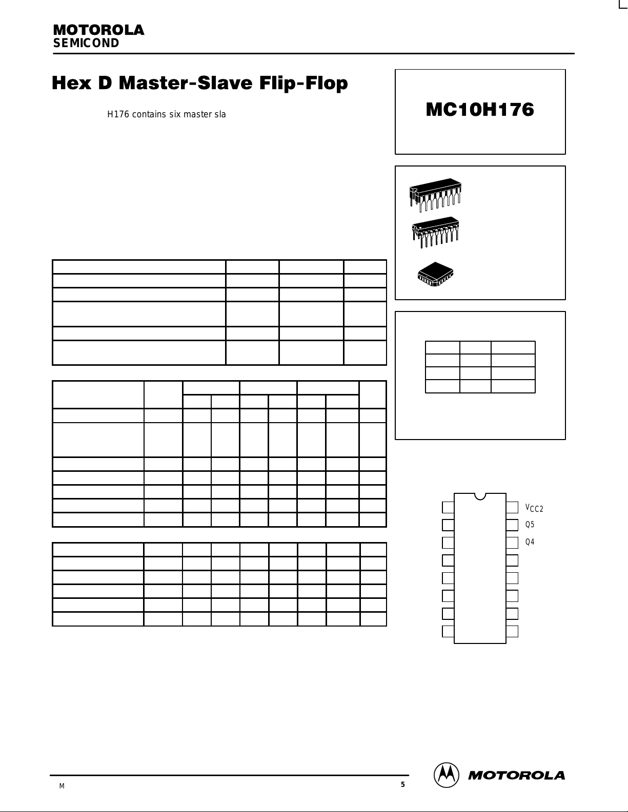
SEMICONDUCTOR TECHNICAL DATA
The MC10H176 contains six master slave type D flip–flops with a common
clock. This MECL 10H part is a functional/pinout duplication of the standard
MECL 10K family part, with 100% improvement in clock frequency and
propagation delay and no increase in power–supply current.
• Propagation Delay, 1.7 ns Typical
• Power Dissipation, 460 mW Typical
• Improved Noise Margin 150 mV (Over Operating Voltage and
Temperature Range)
• Voltage Compensated
• MECL 10K–Compatible
MAXIMUM RATINGS
Characteristic Symbol Rating Unit
Power Supply (VCC = 0) V
Input Voltage (VCC = 0) V
Output Current— Continuous
— Surge
Operating Temperature Range T
Storage Temperature Range— Plastic
— Ceramic
I
T
EE
I
out
A
stg
–8.0 to 0 Vdc
0 to V
EE
50
100
0 to +75 °C
–55 to +150
–55 to +165
Vdc
mA
°C
°C
ELECTRICAL CHARACTERISTICS (VEE = –5.2 V ±5%) (See Note)
0° 25° 75°
Characteristic Symbol Min Max Min Max Min Max Unit
Power Supply Current I
Input Current High
Pins 5,6,7,10,11,12
Pin 9
Input Current Low I
High Output Voltage V
Low Output Voltage V
High Input Voltage V
Low Input Voltage V
I
E
inH
inL
OH
OL
IH
— 123 — 112 — 123 mA
——425
670——
0.5 — 0.5 — 0.3 — µA
–1.02 –0.84 –0.98 –0.81 –0.92 –0.735 Vdc
–1.95 –1.63 –1.95 –1.63 –1.95 –1.60 Vdc
–1.17 –0.84 –1.13 –0.81 –1.07 –0.735 Vdc
–1.95 –1.48 –1.95 –1.48 –1.95 –1.45 Vdc
IL
265
420——
265
420
AC PARAMETERS
Propagation Delay t
Set–up Time t
Hold Time t
Rise Time t
Fall Time t
Toggle Frequency f
NOTE:
Each MECL 10H series circuit has been designed to meet the dc specifications shown in the test
table, after thermal equilibrium has been established. The circuit is in a test socket or mounted on a
printed circuit board and transverse air flow greater than 500 linear fpm is maintained. Outputs are
terminated through a 50–ohm resistor to –2.0 volts.
pd
set
hold
tog
0.9 2.1 0.9 2.2 1.0 2.4 ns
1.5 — 1.5 — 1.5 — ns
0.9 — 0.9 — 1.0 — ns
0.5 1.8 0.5 1.9 0.5 2.0 ns
r
0.5 1.8 0.5 1.9 0.5 2.0 ns
f
250 — 250 — 250 — MHz
µA
L SUFFIX
CERAMIC PACKAGE
CASE 620–10
P SUFFIX
PLASTIC PACKAGE
CASE 648–08
FN SUFFIX
PLCC
CASE 775–02
CLOCKED TRUTH TABLE
C
L
H *
H *
* A clock H is a clock transition from
a low to a high state.
V
CC1
Q0
Q1
Q2
D0
D1
D2
V
EE
Pin assignment is for Dual–in–Line Package.
For PLCC pin assignment, see the Pin Conversion
T ables on page 6–11 of the Motorola MECL Data
Q
X
H
Q
n+1
Q
L
L
H
DIP
PIN ASSIGNMENT
1
2
3
4
5
6
7
8
Book (DL122/D).
16
15
14
13
12
11
10
9
n
V
CC2
Q5
Q4
Q3
D5
D4
D3
CLOCK
3/93
Motorola, Inc. 1996
2–113
REV 5
MC10H176
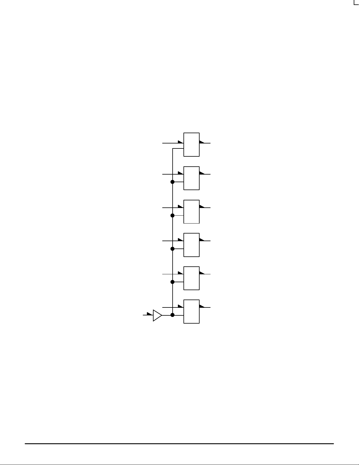
APPLICATION INFORMATION
The MC10H176 contains six high–speed, master slave
type “D” flip–flops. Data is entered into the master when
the clock is low. Master–to–slave data transfer takes
place on the positive–going Clock transition. Thus,
LOGIC DIAGRAM
D0
6D1
7D2
outputs may change only on a positive–going Clock
transition. A change in the information present at the data
(D) input will not affect the output information any other
time due to the master–slave construction of this device.
2 5
Q0
3 Q1
4 Q2
D5
CLOCK 9
10D3
11D4
12
V
CC1
V
CC2
VEE = PIN 8
13 Q3
14 Q4
15 Q5
= PIN 1
= PIN 16
MOTOROLA MECL Data
2–114
DL122 — Rev 6
 Loading...