

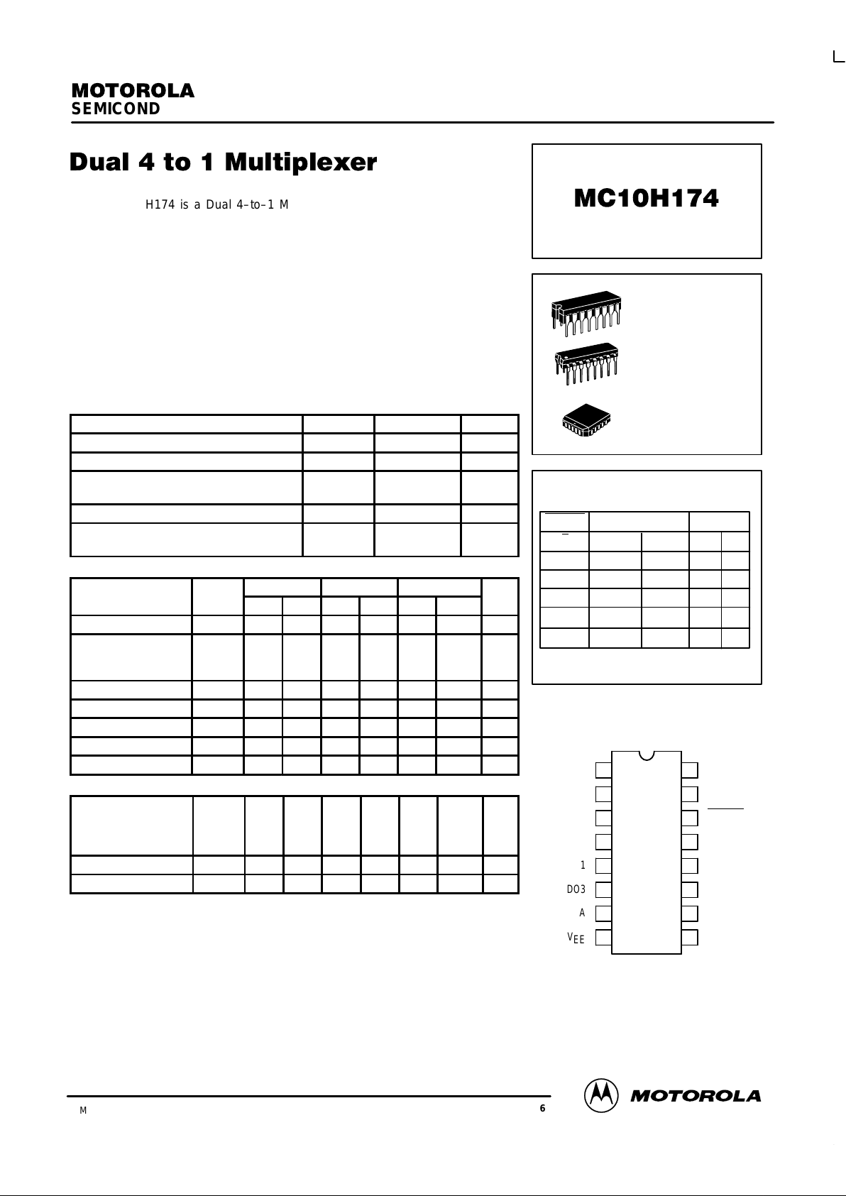
MOTOROLA MC10H174ML1, MC10H174FNR2, MC10H174M, MC10H174MR1, MC10H174ML2 Datasheet
...
SEMICONDUCTOR TECHNICAL DATA
2–73
REV 6
Motorola, Inc. 1996
9/96
The MC10H174 is a Dual 4–to–1 Multiplexer. This device is a functional/
pinout duplication of the standard MECL 10K part, with 100% improvement in
propagation delay and no increase in power supply current.
• Propagation Delay, 1.5 ns Typical
• Power Dissipation, 305 mW Typical
• Improved Noise Margin 150 mV (over operating voltage and
temperature range)
• Voltage Compensated
• MECL 10K–Compatible
MAXIMUM RATINGS
Characteristic Symbol Rating Unit
Power Supply (VCC = 0) V
EE
–8.0 to 0 Vdc
Input Voltage (VCC = 0) V
I
0 to V
EE
Vdc
Output Current— Continuous
— Surge
I
out
50
100
mA
Operating Temperature Range T
A
0 to +75 °C
Storage Temperature Range— Plastic
— Ceramic
T
stg
–55 to +150
–55 to +165
°C
°C
ELECTRICAL CHARACTERISTICS (VEE = –5.2 V ±5%) (See Note)
0° 25° 75°
Characteristic Symbol Min Max Min Max Min Max Unit
Power Supply Current I
E
— 80 — 73 — 80 mA
Input Current High
Pins 3–7 & 9–13
Pin 14
I
inH
——475
670——
300
420——
300
420
µAdc
Input Current Low I
inL
0.5 — 0.5 — 0.3 — µA
High Output Voltage V
OH
–1.02 –0.84 –0.98 –0.81 –0.92 –0.735 Vdc
Low Output Voltage V
OL
–1.95 –1.63 –1.95 –1.63 –1.95 –1.60 Vdc
High Input Voltage V
IH
–1.17 –0.84 –1.13 –0.81 –1.07 –0.735 Vdc
Low Input Voltage V
IL
–1.95 –1.48 –1.95 –1.48 –1.95 –1.45 Vdc
AC PARAMETERS
Propagation Delay
Data
Select (A, B)
Enable
t
pd
0.7
1.0
0.4
2.4
2.8
1.45
0.8
1.1
0.4
2.5
2.9
1.5
0.9
1.2
0.5
2.6
3.2
1.7
ns
Rise Time t
r
0.5 1.5 0.5 1.6 0.5 1.7 ns
Fall Time t
f
0.5 1.5 0.5 1.6 0.5 1.7 ns
NOTE:
Each MECL 10H series circuit has been designed to meet the dc specifications shown in the test table,
after thermal equilibrium has been established. The circuit is in a test socket or mounted on a printed
circuit board and transverse air flow greater than 500 Iinear fpm is maintained. Outputs are terminated
through a 50–ohm resistor to –2.0 volts.
DIP
PIN ASSIGNMENT
V
CC1
Q0
DO0
DO2
DO1
DO3
A
V
EE
V
CC2
Q1
ENABLE
D10
D12
D11
D13
B
16
15
14
13
12
11
10
9
1
2
3
4
5
6
7
8
TRUTH TABLE
ENABLE ADDRESS INPUTS OUTPUTS
X
X
E
BAZW
HLL
LLLX0Y0
LLHX1Y1
LHLX2Y2
LHHX3Y3
L SUFFIX
CERAMIC PACKAGE
CASE 620–10
P SUFFIX
PLASTIC PACKAGE
CASE 648–08
FN SUFFIX
PLCC
CASE 775–02
Pin assignment is for Dual–in–Line Package.
For PLCC pin assignment, see the Pin Conversion
T ables on page 6–11 of the Motorola MECL Data
Book (DL122/D).
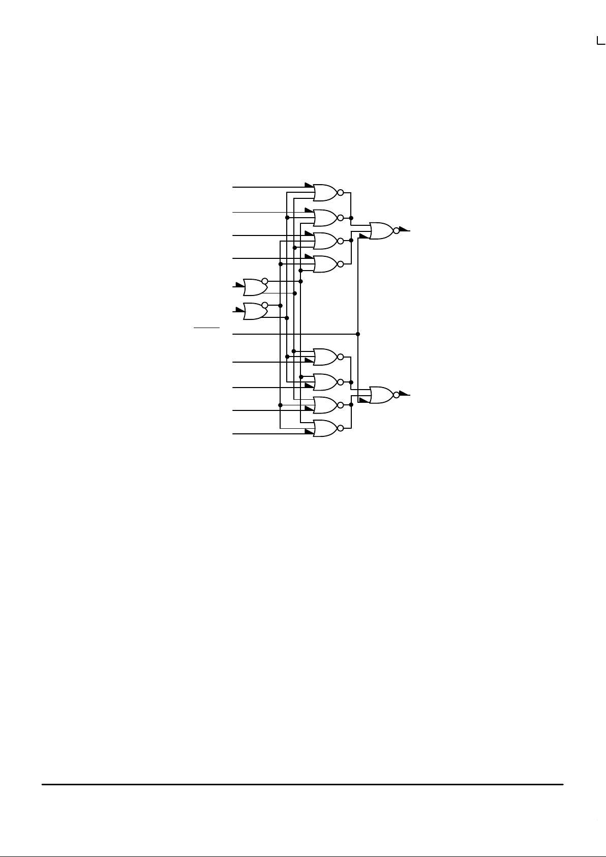
MC10H174
MOTOROLA MECL Data
DL122 — Rev 6
2–74
V
CC1
= PIN 1
V
CC2
= PIN 16
VEE = PIN 8
X0 3
X1 5
X2 4
X3 6
A 7
B9
ENABLE
14
Y0 13
Y1 11
Y2 12
Y3 10
2 Z
15 W
LOGIC DIAGRAM
 Loading...