

Motorola MC10H165FNR2, MC10H165L, MC10H165FN, MC10H165P Datasheet
SEMICONDUCTOR TECHNICAL DATA
The MC10H165 is an 8–Input Priority Encoder. This 10H part is a
functional/pinout duplication of the standard MECL 10K family part, with 100%
improvement in propagation delay, and no increases in power–
supply current.
• Propagation Delay, Data–to–Output, 2.2 ns Typical
• Improved Noise Margin 150 mV (Over Operating Voltage and
Temperature Range)
• Voltage Compensated
• MECL 10K–Compatible
MAXIMUM RATINGS
Characteristic Symbol Rating Unit
Power Supply (VCC = 0) V
Input Voltage (VCC = 0) V
Output Current— Continuous
I
— Surge
Operating Temperature Range T
Storage Temperature Range— Plastic
T
— Ceramic
EE
I
out
A
stg
–8.0 to 0 Vdc
0 to V
EE
50
100
0 to +75 °C
–55 to +150
–55 to +165
Vdc
mA
°C
ELECTRICAL CHARACTERISTICS (VEE = –5.2 V ±5%) (See Note)
0° 25° 75°
Characteristic Symbol Min Max Min Max Min Max Unit
Power Supply Current I
Input Current High
Pin 4
Data Inputs
Input Current Low I
High Output Voltage V
Low Output Voltage V
High Input Voltage V
Low Input Voltage V
I
E
inH
inL
OH
OL
IH
— 144 — 131 — 144 mA
——510
600——
320
370——
0.5 — 0.5 — 0.3 — µA
–1.02 –0.84 –0.98 –0.81 –0.92 –0.735 Vdc
–1.95 –1.63 –1.95 –1.63 –1.95 –1.60 Vdc
–1.17 –0.84 –1.13 –0.81 –1.07 –0.735 Vdc
–1.95 –1.48 –1.95 –1.48 –1.95 –1.45 Vdc
IL
µAdc
320
370
AC PARAMETERS
Propagation Delay
Data Input → Output
Clock Input → Output
Set–up Time t
Hold Time t
Rise Time t
Fall Time t
NOTE:
Each MECL 10H series circuit has been designed to meet the dc specifications shown in the test table,
after thermal equilibrium has been established. The circuit is in a test socket or mounted on a printed circuit
board and transverse air flow greater than 500 Ifpm is maintained. Outputs are terminated through a
50–ohm resistor to –2.0 volts.
t
pd
0.7
3.4
0.7
3.4
0.7
2.2
0.7
3.0 — 3.0 — 3.0 — ns
set
0.5 — 0.5 — 0.5 — ns
hold
0.5 2.4 0.5 2.4 0.5 2.4 ns
r
0.5 2.4 0.5 2.4 0.5 2.4 ns
f
2.2
0.7
0.7
3.4
2.2
ns
L SUFFIX
CERAMIC PACKAGE
CASE 620–10
P SUFFIX
PLASTIC PACKAGE
CASE 648–08
FN SUFFIX
PLCC
CASE 775–02
TRUTH TABLE
DATA INPUTS OUTPUTS
D0
D1
D2
D3
D4
D5
D6
D7
Q3
Q2
Q1
H
X
X
X
X
X
X
X
H
L
L
H
X
X
X
X
X
L
L
H
X
L
L
L
L
L
L
L
L
L
L
L
L
X
L
H
X
L
L
H
L
L
L
L
L
L
L
L
L
L
L
L
X
X
X
X
X
X
X
X
X
X
H
X
X
L
H
X
L
L
H
L
L
L
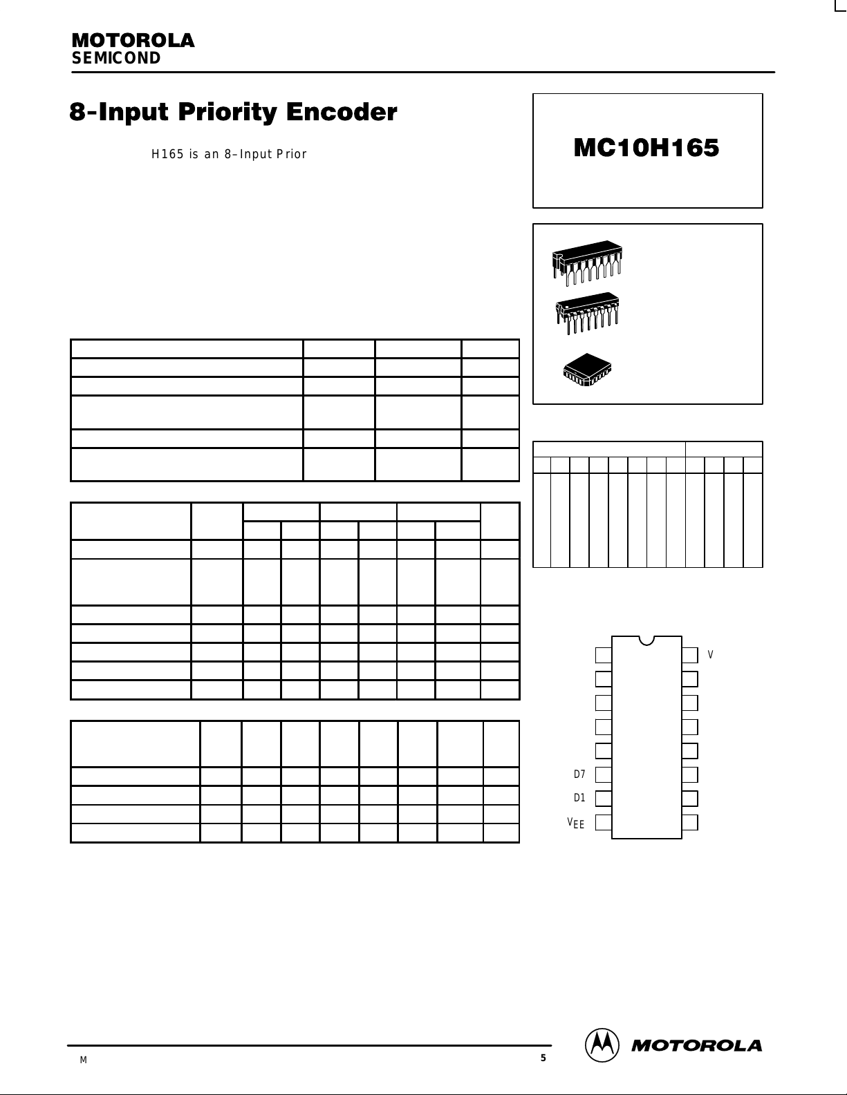
DIP
PIN ASSIGNMENT
V
CC1
Q1
Q0
CLOCK
D0
D7
D1
V
EE
Pin assignment is for Dual–in–Line Package.
For PLCC pin assignment, see the Pin Conversion
T ables on page 6–11 of the Motorola MECL Data
1
2
3
4
5
6
7
8
Book (DL122/D).
16
15
14
13
12
11
10
9
L
H
L
L
H
L
H
H
L
H
H
H
L
H
H
L
H
H
H
H
H
H
L
L
L
V
CC2
Q2
Q3
D2
D5
D4
D3
D6
Q0
L
H
L
H
L
H
L
H
L
3/93
Motorola, Inc. 1996
2–261
REV 5
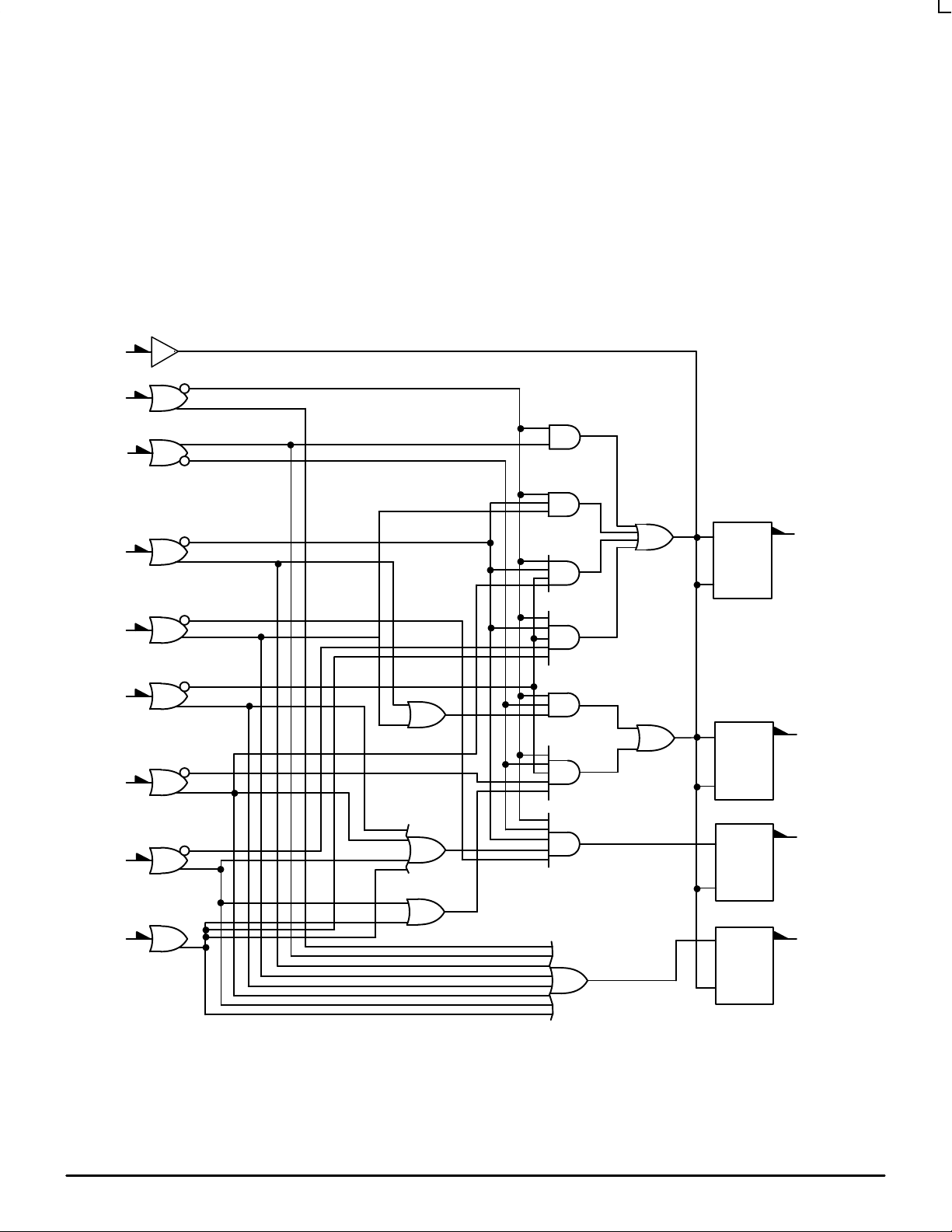
MC10H165
8–INPUT PRIORITY ENCODER
The MC10H165 is a device designed to encode eight
inputs to a binary coded output. The output code is that
of the highest order input. Any input of lower priority is
ignored. Each output incorporates a latch allowing
synchronous operation. When the clock is low the outputs
follow the inputs and latch when the clock goes high. This
device is very useful for a variety of applications in
checking system status in control processors, peripheral
C 4
D0 5
D1 7
D2 13
The input is active when high, (e.g., the three binary
outputs are low when input D0 is high). The Q3 output is
high when any input is high. This allows direct extension
into another priority encoder when more than eight inputs
are necessary. The MC10H165 can also be used to
develop binary codes from random logic inputs, for
addressing ROMs, RAMs, or for multiplexing data.
LOGIC DIAGRAM
controllers, and testing systems.
V
V
VEE= PIN 8.
CC1
CC2
= PIN 1
= PIN 16
3 Q0
D3 10
D4 11
D5 12
D6 9
D7 6
Numbers at ends of terminals denote pin numbers for L and P packages.
2 Q1
15 Q2
14 Q3
MOTOROLA MECL Data
2–262
DL122 — Rev 6
 Loading...