

Motorola MC10H125FN, MC10H125P Datasheet
pp y
SEMICONDUCTOR TECHNICAL DATA
The MC10H125 is a quad translator for interfacing data and control signals
between the MECL section and saturated logic section of digital systems. The
10H part is a functional/pinout duplication of the standard MECL 10K family
part, with 100% improvement in propagation delay, and no increase in
power–supply current.
Outputs of unused translators will go to low state when their inputs are left
open.
• Propagation Delay, 2.5 ns Typical • Voltage Compensated
• Improved Noise Margin 150 mV • MECL 10K–Compatible
(Over Operating Voltage and Temperature Range)
MAXIMUM RATINGS
Characteristic Symbol Rating Unit
Power Supply (VCC = 5.0 V) V
Power Supply (VEE = –5.2 V) V
Input Voltage (VCC = 5.0 V) V
Operating Temperature Range T
Storage Temperature Range — Plastic
— Ceramic
EE
CC
I
A
T
stg
ELECTRICAL CHARACTERISTICS (VEE = –5.2 V ±5%; VCC = 5.0 V ± 5.0 %)
(See Note)
0° 25° 75°
Characteristic Symbol Min Max Min Max Min Max Unit
Negative Power
Supply Drain
Current
Positive Power Supply
Drain Current
Input Current
Input Leakage Current
High Output Voltage
IOH = –1.0 mA
Low Output Voltage
IOL = +20 mA
High Input Voltage(1)
Low Input Voltage(1)
Short Circuit Current
Reference Voltage
Common Mode
Range (3)
Input Sensitivity (4)
I
I
I
V
I
CCH
CCL
I
inH
CBO
V
OH
V
V
V
I
OS
V
CMR
V
E
OL
IH
IL
BB
PP
— 44 — 40 — 44 mA
— 63 — 63 — 63 mA
— 40 — 40 — 40 mA
— 225 — 145 — 145 µA
— 1.5 — 1.0 — 1.0 µA
2.5 — 2.5 — 2.5 — Vdc
— 0.5 — 0.5 — 0.5 Vdc
–1.17 –0.84 –1.13 –0.81 –1.07 –0.735 Vdc
–1.95 –1.48 –1.95 –1.48 –1.95 –1.45 Vdc
60 150 60 150 50 150 mA
–1.38 –1.27 –1.35 –1.25 –1.31 –1.19 Vdc
— — –2.85 to +0.3 V
Typical
150 mV
AC PARAMETERS
Propagation Delay
Rise Time(5)
Fall Time(5)
NOTES:
1. When VBB is used as the reference voltage.
2. Each MECL 10H series circuit has been designed to meet the specifications shown in the test table, after thermal
equilibrium has been established. The circuit is in a test socket or mounted on a printed circuit board and transverse
air flow greater than 500 linear fpm is maintained.
3. Differential input not to exceed 1.0 Vdc.
4. 150 mV
5. 1.0 V to 2.0 V w/25 pF into 500 W.
differential input required to obtain full logic swing on output.
p–p
t
pd
t
t
0.8 3.3 0.85 3.35 0.9 3.4 ns
0.3 1.2 0.3 1.2 0.3 1.2 ns
r
0.3 1.2 0.3 1.2 0.3 1.2 ns
f
–8.0 to 0 Vdc
0 to +7.0 Vdc
0 to V
EE
0 to +75 °C
–55 to +150
–55 to +165
Vdc
°C
°C
L SUFFIX
CERAMIC PACKAGE
CASE 620–10
P SUFFIX
PLASTIC PACKAGE
CASE 648–08
FN SUFFIX
PLCC
CASE 775–02
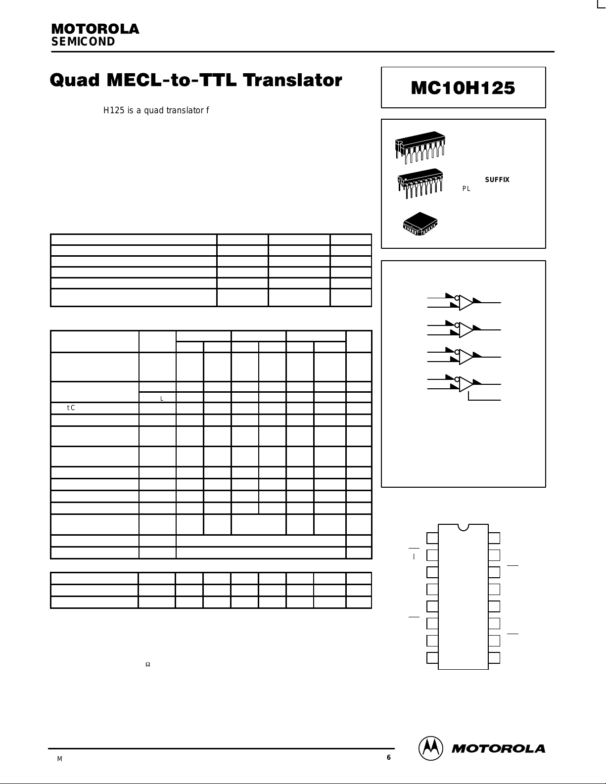
LOGIC DIAGRAM
2
3
6
7
10
11
14
15
VBB*
GND = PIN 16
VCC ( +5.0 VDC)= PIN 9
VEE ( –5.2 VDC) = PIN 8
*VBB to be used to supply bias to the MC10H125
only and bypassed (when used) with 0.01 µF to
0.1 µF capacitor to ground (0 V). VBB can source
< 1.0 mA.
DIP
PIN ASSIGNMENT
V
BB
A
IN
A
IN
A
OUT
B
OUT
B
IN
B
IN
V
EE
Pin assignment is for Dual–in–Line Package.
For PLCC pin assignment, see the Pin Conversion
T ables on page 6–11 of the Motorola MECL Data
1
2
3
4
5
6
7
16
15
14
13
12
11
10
8
Book (DL122/D).
4
5
12
13
1
GND
D
IN
D
IN
D
OUT
C
OUT
C
IN
C
IN
V
9
CC
9/96
Motorola, Inc. 1996
2–29
REV 6

MC10H125
APPLICATION INFORMATION
The MC10H125 incorporates differential inputs and
Schottky TTL “totem pole” outputs. Differential inputs
allow for use as an inverting/non–inverting translator or
as a differential line receiver . The VBB reference voltage
is available on Pin 1 for use in single–ended input biasing.
The outputs of the MC10H125 go to a low–logic level
whenever the inputs are left floating, and a high–logic
output level is achieved with a minimum input level of 150
mV
.
p–p
An advantage of this device is that MECL–level
information can be received, via balanced twisted pair
lines, in the TTL equipment. This isolates the MECL–logic
from the noisy TTL environment. Power supply
requirements are ground, +5.0 volts and –5.2 volts.
MOTOROLA MECL Data
2–30
DL122 — Rev 6
 Loading...