

MOTOROLA MC10H124FNR2, MC10H124M, MC10H124MEL, MC10H124ML1, MC10H124ML2 Datasheet
...
SEMICONDUCTOR TECHNICAL DATA
2–5
REV 6
Motorola, Inc. 1996
9/96
!
!
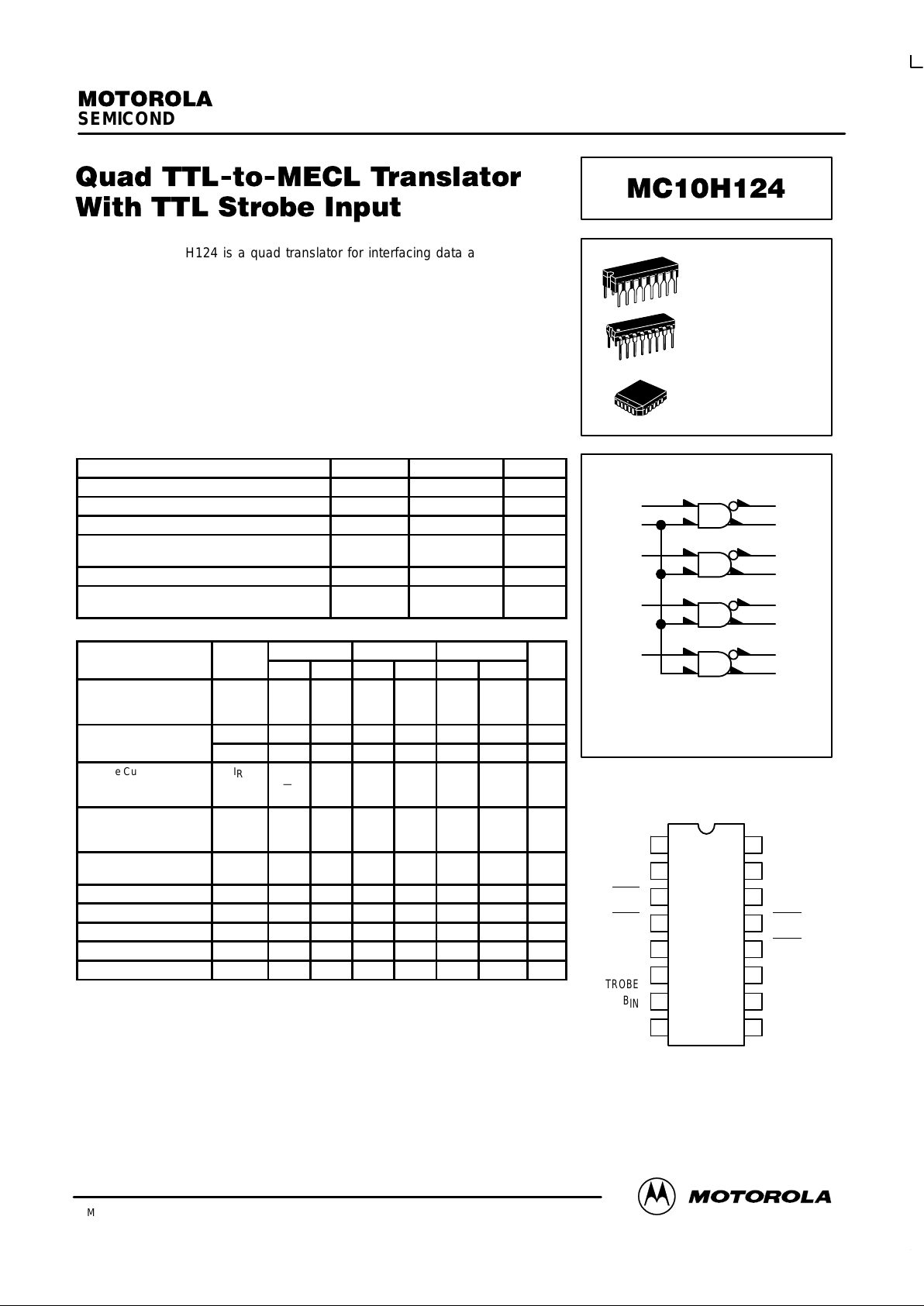
The MC10H124 is a quad translator for interfacing data and control
signals between a saturated logic section and the MECL section of digital
systems. The 10H part is a functional/pinout duplication of the standard
MECL 10K family part, with 100% improvement in propagation delay, and
no increase in power–supply current.
• Propagation Delay, 1.5 ns Typical
• Improved Noise Margin 150 mV (Over Operating Voltage and
Temperature Range)
• Voltage Compensated
• MECL 10K–Compatible
MAXIMUM RATINGS
Characteristic Symbol Rating Unit
Power Supply (VCC = 5.0 V) V
EE
–8.0 to 0 Vdc
Power Supply (VEE = –5.2 V) V
CC
0 to +7.0 Vdc
Input Voltage (VCC = 5.0 V) TTL V
I
0 to V
CC
Vdc
Output Current — Continuous
— Surge
I
out
50
100
mA
Operating T emperature Range T
A
0 to +75 °C
Storage T emperature Range — Plastic
— Ceramic
T
stg
–55 to +150
–55 to +165
°C
ELECTRICAL CHARACTERISTICS (VEE = –5.2 V ±5%, VCC = 5.0 V ± 5.0%)
0° 25° 75°
Characteristic Symbol Min Max Min Max Min Max Unit
Negative Power
Supply Drain
Current
I
E
— 72 — 66 — 72 mA
Positive Power Supply
I
CCH
— 16 — 16 — 18 mA
pp y
Drain Current
I
CCL
— 25 — 25 — 25 mA
Reverse Current
Pin 6
Pin 7
I
R
——20050——20050—
—
200
50
µA
Forward Current
Pin 6
Pin 7
I
F
——–12.8
–3.2——
–12.8
–3.2——
–12.8
–3.2
mA
Input Breakdown
Voltage
V
(BR)in
5.5 — 5.5 — 5.5 — Vdc
Input Clamp Voltage V
I
— –1.5 — –1.5 — –1.5 Vdc
High Output Voltage V
OH
–1.02 –0.84 –0.98 –0.81 –0.92 –0.735 Vdc
Low Output Voltage V
OL
–1.95 –1.63 –1.95 –1.63 –1.95 –1.60 Vdc
High Input Voltage V
IH
2.0 — 2.0 — 2.0 — Vdc
Low Input Voltage V
IL
— 0.8 — 0.8 — 0.8 Vdc
NOTE:
Each MECL 10H series circuit has been designed to meet the dc specifications shown in the test table,
after thermal equilibrium has been established. The circuit is in a test socket or mounted on a printed circuit
board and transverse air flow greater than 500 Ifpm is maintained. Outputs are terminated through a
50–ohm resistor to –2.0 volts.
LOGIC DIAGRAM
DIP
PIN ASSIGNMENT
B
OUT
A
OUT
B
OUT
A
OUT
A
IN
COMMON
STROBE
B
IN
V
EE
GND
C
OUT
D
OUT
D
OUT
C
OUT
D
IN
C
IN
V
CC
16
15
14
13
12
11
10
9
1
2
3
4
5
6
7
8
GND = PIN 16
VCC ( +5.0 VDC) = PIN 9
VEE ( –5.2 VDC) = PIN 8
11
13
14
10
12
15
7
3
1
6
5
4
2
L SUFFIX
CERAMIC PACKAGE
CASE 620–10
P SUFFIX
PLASTIC PACKAGE
CASE 648–08
FN SUFFIX
PLCC
CASE 775–02
Pin assignment is for Dual–in–Line Package.
For PLCC pin assignment, see the Pin Conversion
T ables on page 6–36 of the Motorola MECL Data
Book (DL122/D).
MC10H124
MOTOROLA MECL Data
DL122 — Rev 6
2–6
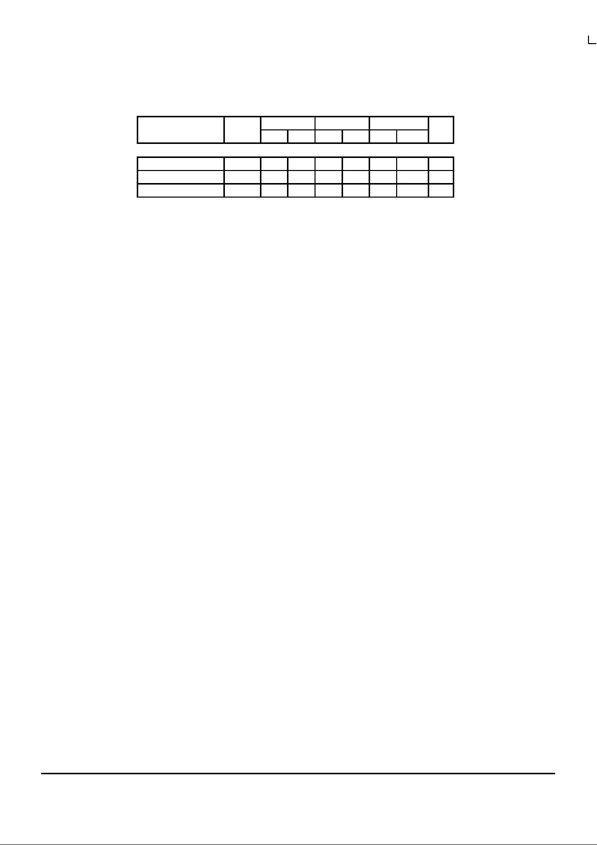
ELECTRICAL CHARACTERISTICS (VEE = –5.2 V ±5%, VCC = 5.0 V ± 5.0%)
0° 25° 75°
Characteristic Symbol Min Max Min Max Min Max Unit
AC PARAMETERS
Propagation Delay t
pd
0.55 2.25 0.55 2.4 0.85 2.95 ns
Rise Time t
r
0.5 1.5 0.5 1.6 0.5 1.7 ns
Fall Time t
f
0.5 1.5 0.5 1.6 0.5 1.7 ns
APPLICATIONS INFORMATION
The MC10H124 has TTL–compatible inputs and
MECL complementary open–emitter outputs that allow
use as an inverting/non–inverting translator or as a
differential line driver. When the common strobe input is
at the low–logic level, it forces all true outputs to a MECL
low–logic state and all inverting outputs to a MECL
high–logic state.
An advantage of this device is that TTL–level
information can be transmitted differentially , via balanced
twisted pair lines, to MECL equipment, where the signal
can be received by the MC10H115 or MC10H116
differential line receivers. The power supply
requirements are ground, +5.0 volts, and –5.2 volts.
 Loading...