

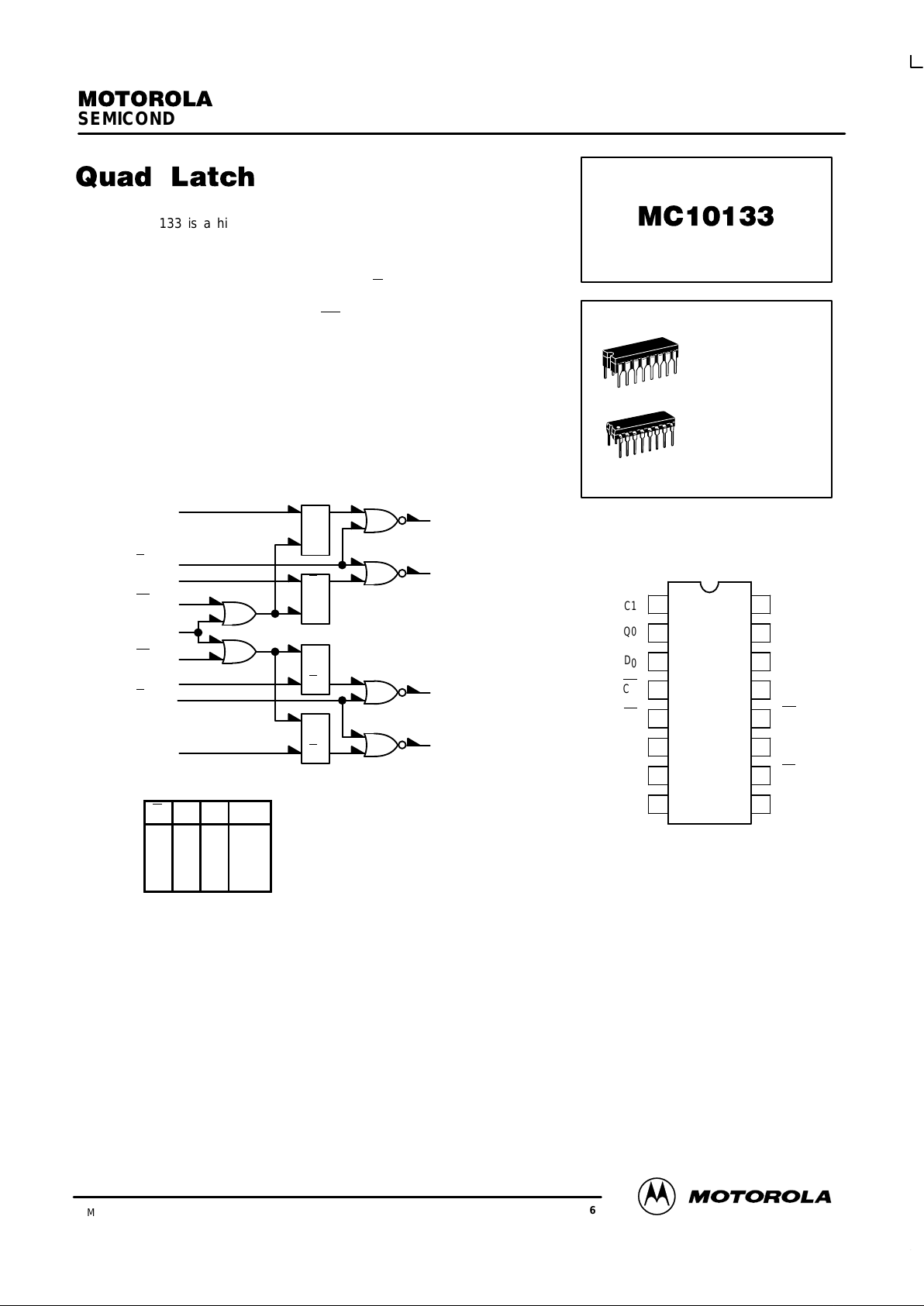
LOGIC DIAGRAM
V
CC1
= PIN 1
V
CC2
= PIN 16
VEE= PIN 8
Q0
Q
1
Q
2
Q
3
3D0
2Q0
5G
0
7D1
4CE
13C
C
12CE
9D2
14D3
6Q1
11 Q2
15 Q3
10G
1
SEMICONDUCTOR TECHNICAL DATA
3–13
REV 6
Motorola, Inc. 1996
9/96
The MC10133 is a high speed, low power, quad latch consisting of four
bistable latch circuits with D type inputs and gated Q outputs, allowing direct
wiring to a bus. When the clock is high, outputs will follow D inputs. Information
is latched on the negative going transition of the clock.
The outputs are gated when the output enable (G
) is low. All four latches may
be clocked at one time with the common clock (CC), or each half may be
clocked separately with its clock enable (CE
).
PD= 310 mW typ/pkg (No Load)
tpd= 4.0 ns typ
tr, tf= 2.0 ns typ (20%–80%)
TRUTH TABLE
G C D Q
n+1
H X X L
L L X Q
n
L H L L
L H H H
C = CC + CE
DIP
PIN ASSIGNMENT
V
CC1
Q0
D
0
CE
G0
Q1
D1
V
EE
V
CC2
Q3
D3
C
C
CE
Q2
G1
D2
16
15
14
13
12
11
10
9
1
2
3
4
5
6
7
8
L SUFFIX
CERAMIC PACKAGE
CASE 620–10
P SUFFIX
PLASTIC PACKAGE
CASE 648–08
MC10133
MOTOROLA MECL Data
DL122 — Rev 6
3–14
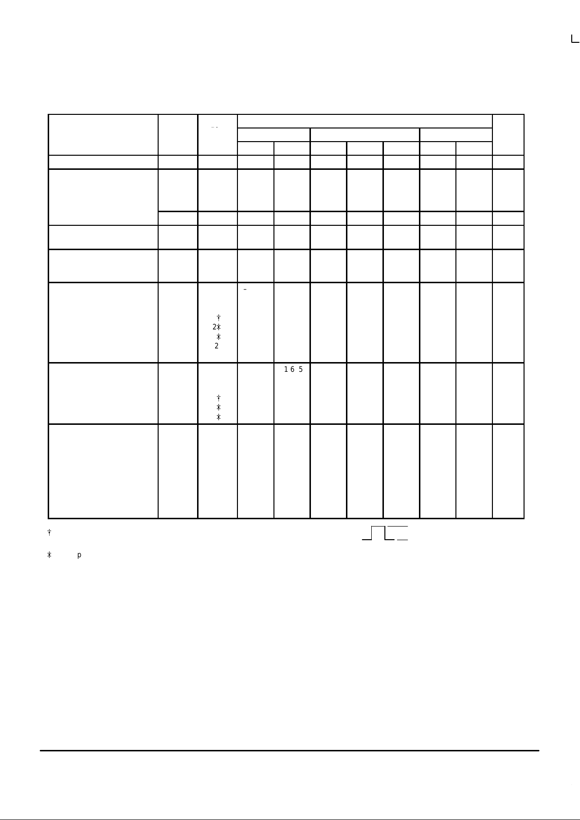
ELECTRICAL CHARACTERISTICS
Test Limits
Pin
Under
–30°C +25°C +85°C
Characteristic Symbol
Under
Test
Min Max Min Typ Max Min Max
Unit
Power Supply Drain Current I
E
8 82 75 82 mAdc
Input Current I
inH
3
4
5
13
390
425
560
560
245
265
350
350
245
265
350
350
µAdc
I
inL
3 0.5 0.5 0.3 µAdc
Output Voltage Logic 1 V
OH
2
2
–1.060
–1.060
–0.890
–0.890
–0.960
–0.960
–0.810
–0.810
–0.890
–0.890
–0.700
–0.700
Vdc
Output Voltage Logic 0 V
OL
2
2
2
–1.890
–1.890
–1.890
–1.675
–1.675
–1.675
–1.850
–1.850
–1.850
–1.650
–1.650
–1.650
–1.825
–1.825
–1.825
–1.615
–1.615
–1.615
Vdc
Threshold Voltage Logic 1 V
OHA
2
2
2
2
[
2
]
2
]
2
2
–1.080
–1.080
–1.080
–1.080
–1.080
–1.080
–1.080
–1.080
–0.980
–0.980
–0.980
–0.980
–0.980
–0.980
–0.980
–0.980
–0.910
–0.910
–0.910
–0.910
–0.910
–0.910
–0.910
–0.910
Vdc
Threshold Voltage Logic 0 V
OLA
2
2
2
2
[
2
]
2
]
–1.655
–1.655
–1.655
–1.655
–1.655
–1.655
–1.630
–1.630
–1.630
–1.630
–1.630
–1.630
–1.595
–1.595
–1.595
–1.595
–1.595
–1.595
Vdc
Switching Times (50Ω Load) ns
Propagation Delay t
3+2+
t
4+2+
t
5–2+
t
setup
t
hold
2
2
2
3
3
1.0
1.0
1.0
2.5
1.5
5.6
5.4
3.2
1.0
1.0
1.0
2.5
1.5
4.0
4.0
2.0
0.7
0.7
5.4
5.4
3.1
1.1
1.2
1.0
2.5
1.5
5.9
6.0
3.4
Rise Time (20 to 80%) t
2+
2 1.0 3.6 1.1 2.0 3.5 1.1 3.8
Fall Time (20 to 80%) t
2–
2 1.0 3.6 1.1 2.0 3.5 1.1 3.8
[
Output level to be measured after a clock pulse has been applied to the clock input (Pin 4)
V
IHmax
V
ILmin
]
Data input at proper high/low level while clock pulse is high so that device latches ar proper high/low level for test. Levels are measured after
device has latched.
* Latch set to zero state before test.
 Loading...