

Motorola MC10131P, MC10131FN Datasheet
SEMICONDUCTOR TECHNICAL DATA
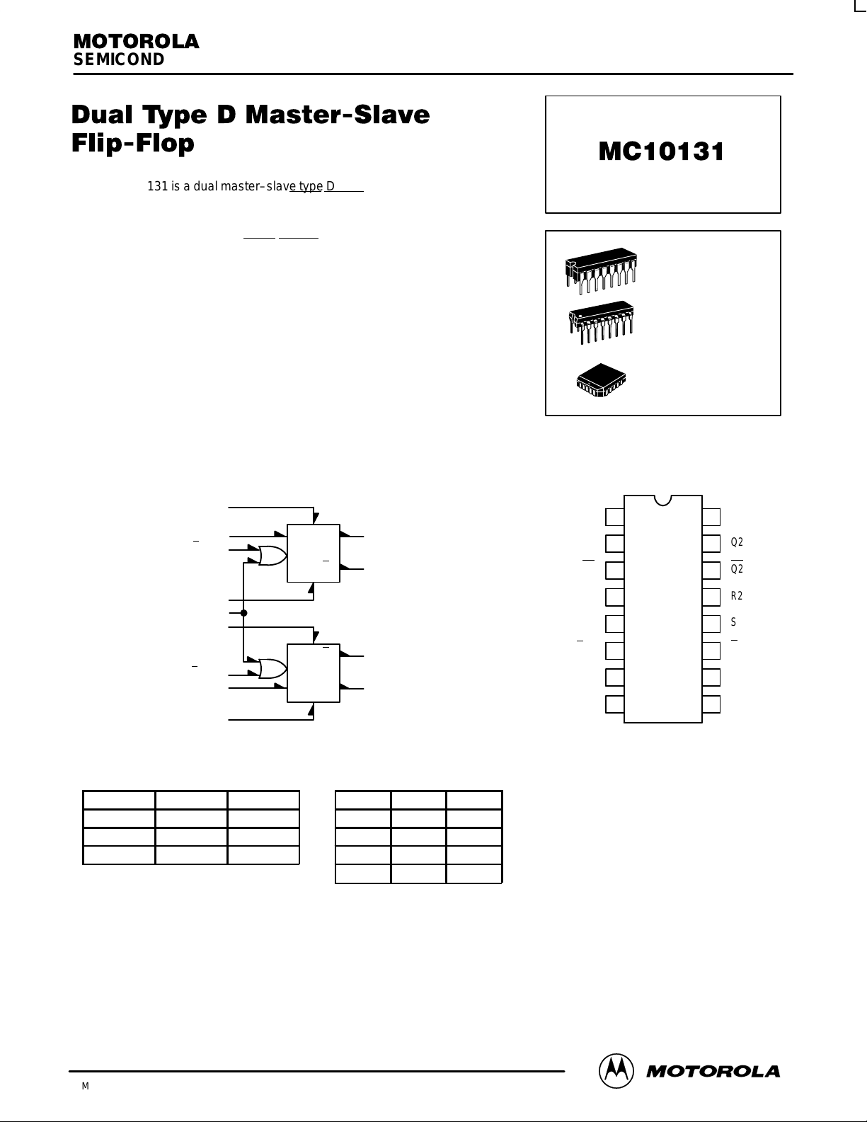
The MC10131 is a dual master–slave type D flip–flop. Asynchronous Set (S)
and Reset (R) override Clock (CC) and Clock
may be clocked separately by holding the common clock in the low state and
using the enable inputs for the clocking function. If the common clock is to be
used to clock the flip–flop, the Clock
Enable inputs must be in the low state. In
this case, the enable inputs perform the function of controlling the common
clock.
The output states of the flip–flop change on the positive transition of the
clock. A change in the information present at the data (D) input will not affect the
output information at any other time due to master slave construction.
PD= 235 mW typ/pkg (No Load)
F
= 160 MHz typ
Tog
tpd= 3.0 ns typ
tr, tf= 2.5 ns typ (20%–80%)
LOGIC DIAGRAM
S1 5
D1 7
C
6
E1
Enable (CE) inputs. Each flip–flop
Q1
Q
1
2
3
DIP
PIN ASSIGNMENT
V
CC1
Q1
Q1
1
2
3
L SUFFIX
CERAMIC PACKAGE
CASE 620–10
P SUFFIX
PLASTIC PACKAGE
CASE 648–08
FN SUFFIX
PLCC
CASE 775–02
16
15
14
V
Q2
Q2
CC2
R1 4
CC 9
R2 13
14
15
V
CC1
V
CC2
VEE= PIN 8
C
E2
D2 10
S2 12
11
Q
Q2
2
CLOCKED TRUTH TABLE R–S TRUTH TABLE
C D Q
L X Q
H L L L H H
H H H H L L
C = CE + CC.A clock H is a clock transition from a
low to a high state.
n+1
n
R S Q
L L Q
H H N.D.
N.D. = Not Defined
= PIN 1
= PIN 16
n+1
R1
S1
C
E1
D1
V
EE
Pin assignment is for Dual–in–Line Package.
For PLCC pin assignment, see the Pin Conversion
T ables on page 6–11 of the Motorola MECL Data
n
4
5
6
7
8
Book (DL122/D).
13
12
11
10
9
R2
S2
C
D2
C
E2
C
3/93
Motorola, Inc. 1996
3–8
REV 5

MC10131
Under
ELECTRICAL CHARACTERISTICS
Test Limits
Pin
Characteristic Symbol
Power Supply Drain Current I
Input Current I
Output Voltage Logic 1 V
Output Voltage Logic 0 V
Threshold Voltage Logic 1 V
Threshold Voltage Logic 0 V
Switching Times (50Ω Load)
Clock Input
Propagation Delay t
Rise Time (20 to 80%) t
Fall Time (20 to 80%) t
Set Input ns
Propagation Delay t
Reset Input ns
Propagation Delay t
Setup Time t
Hold Time t
Toggle Frequency (Max) f
* Individually test each input applying VIH or VIL to input under test.
[
Output level to be measured after a clock pulse has been applied to the C
E
inH
I
inL
OH
OL
OHA
OLA
9+2–
t
9+2+
t
6+2+
t
6+2–
2+
2–
5+2+
t
12+15+
t
5+3–
t
12+14–
4+2–
t
13+15–
t
4+3–
t
13+14+
setup
hold
tog
Under
Test
8 62 45 56 62 mAdc
4
5
6
7
9
4, 5*
6, 7, 9*
2
2
[
2
3
[
2
2
[
2
3
[
2
2
2
2
2 1.0 4.6 1.1 2.5 4.5 1.1 4.9
2 1.0 4.6 1.1 2.5 4.5 1.1 4.9
2
15
3
14
2
15
3
14
7 2.5 2.5 2.5 ns
7 1.5 1.5 1.5 ns
2 125 125 160 125 MHz
–30°C +25°C +85°C
Min Max Min Typ Max Min Max
0.5
0.5
–1.060
–1.060
–1.890
–1.890
–1.080
–1.080
1.7
1.7
1.7
1.7
1.7
1.7
1.7
1.7
1.7
1.7
1.7
1.7
525
525
350
390
425
–0.890
–0.890
–1.675
–1.675
–1.655
–1.655
4.6
4.6
4.6
4.6
4.4
4.4
4.4
4.4
4.4
4.4
4.4
4.4
0.5
0.5
–0.960
–0.960
–1.850
–1.850
–0.980
–0.980
1.8
1.8
1.8
1.8
1.8
1.8
1.8
1.8
1.8
1.8
1.8
1.8
Input (Pin 6)
E
3.0
3.0
3.0
3.0
2.8
2.8
2.8
2.8
2.8
2.8
2.8
2.8
330
330
220
245
265
–0.810
–0.810
–1.650
–1.650
–1.630
–1.630
4.5
4.5
4.5
4.5
4.3
4.3
4.3
4.3
4.3
4.3
4.3
4.3
V
V
IHmax
ILmin
0.3
0.3
–0.890
–0.890
–1.825
–1.825
–0.910
–0.910
1.8
1.8
1.8
1.8
1.8
1.8
1.8
1.8
1.8
1.8
1.8
1.8
–0.700
–0.700
–1.615
–1.615
–1.595
–1.595
330
330
220
245
265
5.0
5.0
5.0
5.0
4.8
4.8
4.8
4.8
4.8
4.8
4.8
4.8
Unit
µAdc
µAdc
Vdc
Vdc
Vdc
Vdc
ns
DL122 — Rev 6
3–9 MOTOROLAMECL Data
 Loading...