

Motorola MC10129L Datasheet
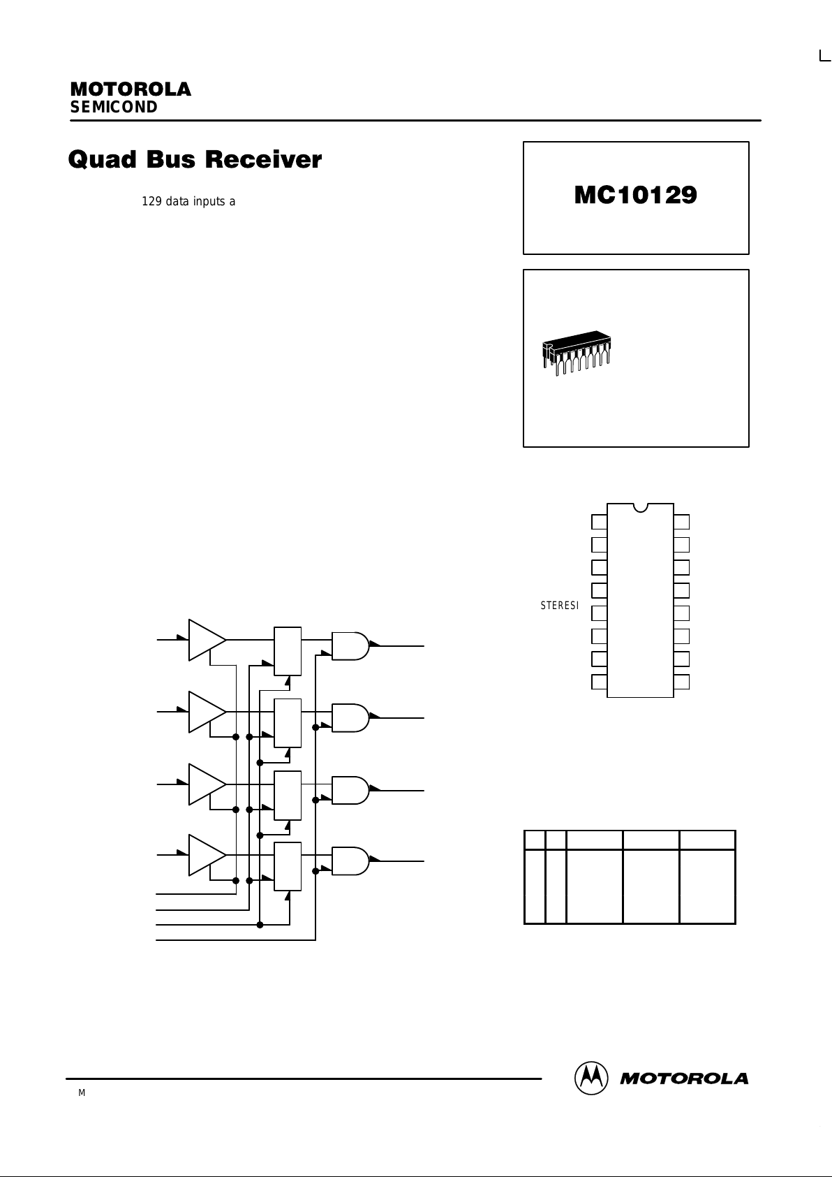
LOGIC DIAGRAM
VCC = PIN 9
GND = PIN 1 AND 16
VEE = PIN 8
14 Q0
D0 7
D
C
R
15 Q1
D1 13
D
C
R
3Q2
D2 6
D
C
R
2Q3
D3 4
D
C
R
HYSTERESIS
CONTROL 5
CLOCK 11
RESET 10
STROBE 12
SEMICONDUCTOR TECHNICAL DATA
3–1
REV 6
Motorola, Inc. 1996
9/96
The MC10129 data inputs are compatible with, and accept TTL logic levels
as well as levels compatible with IBM–type buses. The clock, strobe, and reset
inputs accept MECL 10,000 logic levels.
The data inputs accept the bus levels, and storage elements are provided to
yield temporary latch storage of the information after receiving it from the bus.
The outputs can be strobed to allow accurate synchronization of signals and/or
connection to MECL 10,000 level buses. When the clock is low, and the reset
input is disabled, the outputs will follow the D inputs. The latches will store the
data on the rising edge of the clock. The outputs are enabled when the strobe
input is high. Unused D inputs must be tied to VCC or Gnd. The clock, strobe,
and reset inputs each have 50 k ohm pulldown resistors to VEE. They may be
left floating, if not used.
The MC10129 will operate in either of two modes. The first mode is obtained
by tying the hysteresis control input to VEE. In this mode, the input threshold
points of the D inputs are fixed. The second mode is obtained by tying the
hysteresis control input to ground. In this mode, input hysteresis is achieved as
shown in the test table. This hysteresis is desirable where extra noise margin is
required on the D inputs. The outer input pins are unaffected by the mode of
operation used.
The MC10129 is especially useful in interface applications for central
processors, mini–computers, and peripheral equipment.
PD= 750 mW typ/pkg (No Load)
tpd= 10 ns typ
VCC Max = 7.0 Vdc
TRUTH TABLE
D C STROBE RESET Qn +
1
X X L X L
X H X H L
L L H X L
X H H L Q
n
H L H X H
PIN ASSIGNMENT
GND
Q3
Q2
D3
HYSTERESIS
CONTROL
D2
D0
V
EE
GND
Q1
Q0
D1
STROBE
CLOCK
RESET
V
CC
16
15
14
13
12
11
10
9
1
2
3
4
5
6
7
8
L SUFFIX
CERAMIC PACKAGE
CASE 620–10
MC10129
MOTOROLA MECL Data
DL122 — Rev 6
3–2
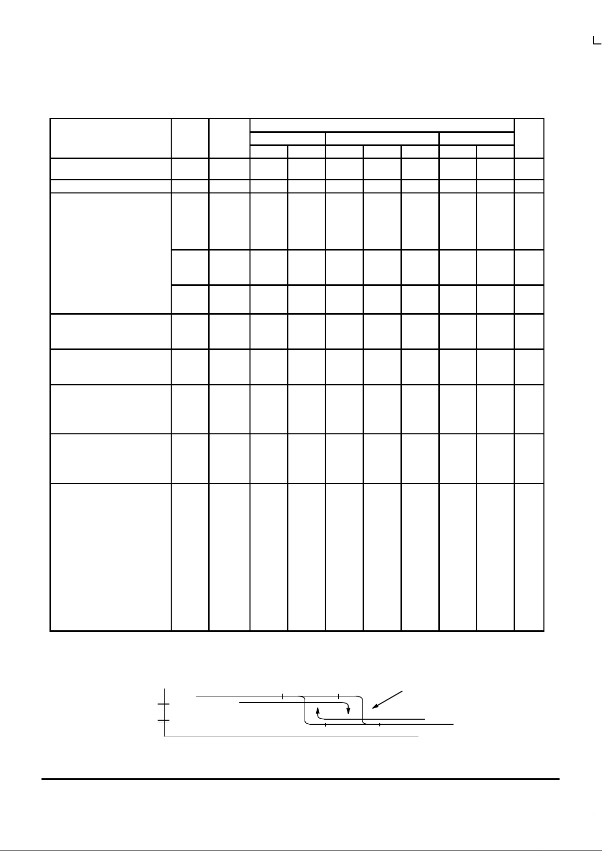
ELECTRICAL CHARACTERISTICS
Test Limits
Pin
Under
–30°C +25°C +85°C
Characteristic Symbol
Under
Test
Min Max Min Typ Max Min Max
Unit
Negative Power Supply Drain
Current
I
E
8
8
167
189
152
172
167
189
mAdc
Positive Power Supply Drain Current I
CC
9 8.0 8.0 8.0 mAdc
Input Current I
inH
4
6
7
10
11
12
13
150
150
150
720
390
390
150
95
95
95
450
245
245
95
95
95
95
450
245
245
95
µAdc
I
CBO
(1.) 4
6
7
13
1.5
1.5
1.5
–1.0
–1.0
–1.0
–1.0
1.0
1.0
1.0
µAdc
I
inL
10
11
12
0.5
0.5
0.5
0.5
0.5
0.5
0.3
0.3
0.3
µAdc
Output Voltage Logic 1 V
OH
2
3
2
3
–1.060
–1.060
–1.060
–1.060
–0.890
–0.890
–0.890
–0.890
–0.960
–0.960
–0.960
–0.960
–0.810
–0.810
–0.810
–0.810
–0.890
–0.890
–0.890
–0.890
–0.700
–0.700
–0.700
–0.700
Vdc
Output Voltage Logic 0 V
OL
2
3
2
3
–1.890
–1.890
–1.890
–1.890
–1.675
–1.675
–1.675
–1.675
–1.850
–1.850
–1.850
–1.850
–1.650
–1.650
–1.650
–1.650
–1.825
–1.825
–1.825
–1.825
–1.615
–1.615
–1.615
–1.615
Vdc
Threshold Voltage Logic 1 V
OHA
2 (2.)
2
2
2
2
(3.)
2 (4.)
–1.080
–1.080
–1.080
–1.080
–1.080
–1.080
–0.980
–0.980
–0.980
–0.980
–0.980
–0.980
–0.910
–0.910
–0.910
–0.910
–0.910
–0.910
Vdc
Threshold Voltage Logic 0 V
OLA
2 (2.)
2
2
(2.)
2
2
(3.)
2 (4.)
–1.655
–1.655
–1.655
–1.655
–1.655
–1.655
–1.630
–1.630
–1.630
–1.630
–1.630
–1.630
–1.595
–1.595
–1.595
–1.595
–1.595
–1.595
Vdc
Switching Times
Propagation Delay
ns
Data Input t
7+14+
t
7–14–
14
14
3.7
3.7
15
15
3.7
3.7
10
10
15
15
3.7
3.7
30
40
Clock Input t
11–14+
t
11–14–
14
14
2.7
2.7
11
11
2.7
2.7
5.0
5.0
9.0
9.0
2.7
2.7
11
11
Strobe Input t
12+14+
t
12–14–
14
14
1.6
1.6
8.0
8.0
1.6
1.6
4.0
4.0
7.0
7.0
1.6
1.6
8.0
8.0
Reset Input t
10+14–
14 2.0 8.0 2.0 5.0 6.5 2.0 8.0
Hysteresis Mode t
7+14+
t
7–14–
14
14
6.6
3.7
30
17
6.7
3.7
18
10
25
15
6.6
3.7
30
40
Setup Time t
setup
14 30 2.7 15 30
Hold Time t
hold
14 0 –2.0 15 –2.0
Rise Time t+ 14 1.5 5.0 1.5 2.0 4.3 1.5 5.0
Fall Time t– 14 1.5 5.0 1.5 2.0 4.3 1.5 5.0
1. Pin 5 to VEE, VIL to Data input one at a time.
2. Output latched to logic high state prior to test. V
IHA
′, V
ILA
′ are standard logic 1 and logic 0 MTTL threshold voltages. V
IHA
′′, V
ILA
′′, V
IHA
′′′ and V
ILA
′′′ are logic 1 and
logic 0 threshold voltages in the hysteresis mode as shown in Figure 1 on page 3–2.
3. Input level on data input taken from +0.4V up to voltage level given.
4. Input level on data input taken from +4.0V down to voltage level given.
5. Operation and limits shown also apply for VCC = +6.0V.
V
in
V
out
Logic 1
Logic 0
V
IHA
′′
V
IHA
′′′
V
ILA
′′
V
ILA
′′′
Hysteresis Mode
Threshold Voltage
Figure 1. Hysteresis Mode Threshold Voltage
MC10129
3–3 MOTOROLAMECL Data
DL122 — Rev 6
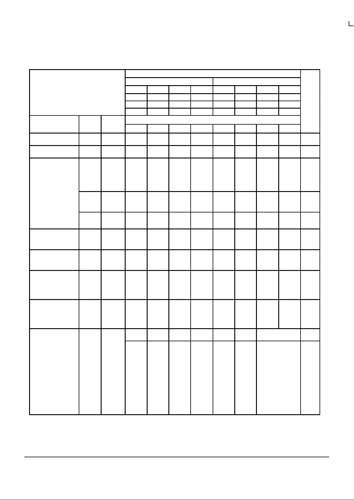
ELECTRICAL CHARACTERISTICS
TEST VOLTAGE VALUES (Volts)
MECL 10,000 INPUT LEVELS TTL INPUT LEVELS (6.)
@ Test Temperature V
IHmaxVILminVIHAminVILAmax
V
IH
V
IL
V
IHA′
V
ILA′
–30°C –0.890 –1.890 –1.155 –1.500 3.000 0.400 2.000 0.800
+25°C –0.810 –1.850 –1.105 –1.475 3.000 0.400 2.000 0.800
+85°C –0.700 –1.825 –1.035 –1.440 3.000 0.400 2.000 0.800
Pin
TEST VOLTAGE APPLIED TO PINS LISTED BELOW
Characteristic Symbol
Und
er
Test
V
IHmaxVILminVIHAminVILAmax
V
IH
V
IL
V
IHA′
V
ILA′
Gnd
Negative Power Supply
Drain Current
I
E
8
8
11
11
12
12
1,5,16
1,16
Positive Power Supply
Drain Current
I
CC
9 4,6,7,13 1,16
Input Current I
inH
4
6
7
10
11
12
13
10,11
11
12
4
6
7
13
1,16
1,16
1,16
1,16
1,16
1,16
1,16
I
CBO
(1.) 4
6
7
13
4
6
7
13
1,16
1,16
1,16
1,16
I
inL
10
11
12
10
11
12
1,16
1,16
1,16
Output Voltage
Logic 1
V
OH
2
3
2
3
12
12
12
12
10,11
10,11
10,11
10,11
4
6
4
6
1,16
1,16
1,5,16
1,5,16
Output Voltage
Logic 0
V
OL
2
3
2
3
12
12
12
12
10,11
10,11
10,11
10,11
4
6
4
6
1,16
1,16
1,5,16
1,5,16
Threshold Voltage
Logic 1
V
OHA
2 (2.)
2
2
2
2
(3.)
2 (4.)
11,12
10,12
12
12
12
10,11
10,11
10,11
10,11
12
10
11
4
4
4
4
1,16
1,16
1,16
1,16
1,5,16
1,5,16
Threshold Voltage
Logic 0
V
OLA
2 (2.)
2
2
(2.)
2
2
(3.)
2 (4.)
11,12
10,12
12
12
12
10,11
10,11
10,11
10,11
10
11
12
4
4
4
4
1,16
1,16
1,16
1,16
1,5,16
1,5,16
Switching Times
Propagation Delay
+1.11V +0.31V Pulse In
Pulse
Out
+5.0V +2.40V Figure +2.0V
Data Input t
7+14+
t
7–14–
14
14
12
12
10,11
10,11
7
7
14
14
Figure 3
Figure 3
1,16
1,16
Clock Input t
11–14+
t
11–14–
14
14
12
12
10
10
7,11
7,11
14
14
Figure 6
Figure 6
1,16
1,16
Strobe Input t
12+14+
t
12–14–
14
14
10,11
10,11
12
12
14
14
7
7
Figure 4
Figure 4
1,16
1,16
Reset Input t
10+14–
14 12 10,11 14 7 7 Figure 5 1,16
Hysteresis Mode t
7+14+
t
7–14–
14
14
12
12
10,11
10,11
7
7
14
14
Figure 3
Figure 3
1,5,16
1,5,16
Setup Time t
setup
14 12 10 7,1 1 14 Figure 7 1,16
Hold Time t
hold
14 12 10 7,11 14 Figure 7 1,16
Rise Time t+ 14 12 10,11 7 14 Figure 3 1,16
Fall Time t– 14 12 10,11 7 14 Figure 3 1,16
1. Pin 5 to VEE, VIL to Data input one at a time.
2. Output latched to logic high state prior to test. V
IHA
′, V
ILA
′ are standard logic 1 and logic 0 MTTL threshold voltages. V
IHA
′′, V
ILA
′′, V
IHA
′′′ and V
ILA
′′′ are logic 1 and
logic 0 threshold voltages in the hysteresis mode as shown in Figure 1 on page 3–2.
3. Input level on data input taken from +0.4V up to voltage level given.
4. Input level on data input taken from +4.0V down to voltage level given.
5. Operation and limits shown also apply for VCC = +6.0V. 6. When testing, choose either TTL or IBM input levels.
 Loading...