

SEMICONDUCTOR TECHNICAL DATA
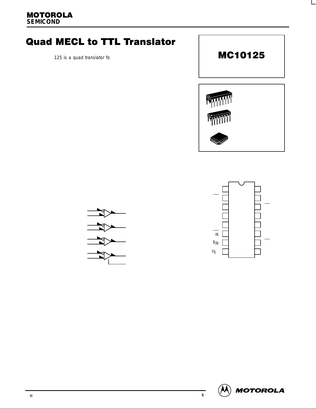
The MC10125 is a quad translator for interfacing data and control signals
between the MECL section and saturated logic sections of digital systems. The
MC10125 incorporates differential inputs and Schottky TTL “totem pole”
outputs. Differential inputs allow for use as an inverting/ non–inverting translator
or as a differential line receiver . The VBB reference voltage is available on pin 1
for use in single–ended input biasing. The outputs of the MC10125 go to a low
logic level whenever the inputs are left floating.
Power supply requirements are ground, +5.0 Volts and –5.2 Volts.
Propagation delay of the MC10125 is typically 4.5 ns. The MC10125 has fanout
of 10 TTL loads. The dc levels are MECL 10,000 in and Schottky TTL, or TTL
out. This device has an input common mode noise rejection of
± 1.0 Volt.
An advantage of this device is that MECL level information can be received,
via balanced twisted pair lines, in the TTL equipment. This isolates the MECL
logic from the noisy TTL environment. This device is useful in computers,
instrumentation, peripheral controllers, test equipment and digital
communications systems.
PD= 380 mW typ/pkg (No Load)
tpd= 4.5 ns typ (50% to + 1.5 Vdc out)
tr, tf= 2.5 ns typ (1.0 V to 2.0 V)
LOGIC DIAGRAM
2
3
6
7
10
11
14
15
VBB*
Gnd = PIN 16
VCC (+5.0Vdc) = PIN 9
VEE (–5.2Vdc) = PIN 8
4
5
12
13
1
L SUFFIX
CERAMIC PACKAGE
CASE 620–10
P SUFFIX
PLASTIC PACKAGE
CASE 648–08
FN SUFFIX
PLCC
CASE 775–02
DIP
PIN ASSIGNMENT
V
BB
A
IN
A
IN
A
OUT
B
OUT
B
IN
B
IN
V
EE
Pin assignment is for Dual–in–Line Package.
For PLCC pin assignment, see the Pin Conversion
T ables on page 6–11 of the Motorola MECL Data
1
2
3
4
5
6
7
8
Book (DL122/D).
16
15
14
13
12
11
10
GND
D
IN
D
IN
D
OUT
C
OUT
C
IN
C
IN
V
9
CC
*VBB to be used to supply bias to the MC10125 only and bypassed (when used)
with 0.01 µF to 0.1 µF capacitor to ground (0 V). VBB can source < 1.0 mA.
When the input pin with the bubble goes positive, the output goes negative.
3/93
Motorola, Inc. 1996
3–89
REV 5
MC10125
Under
pp y
p
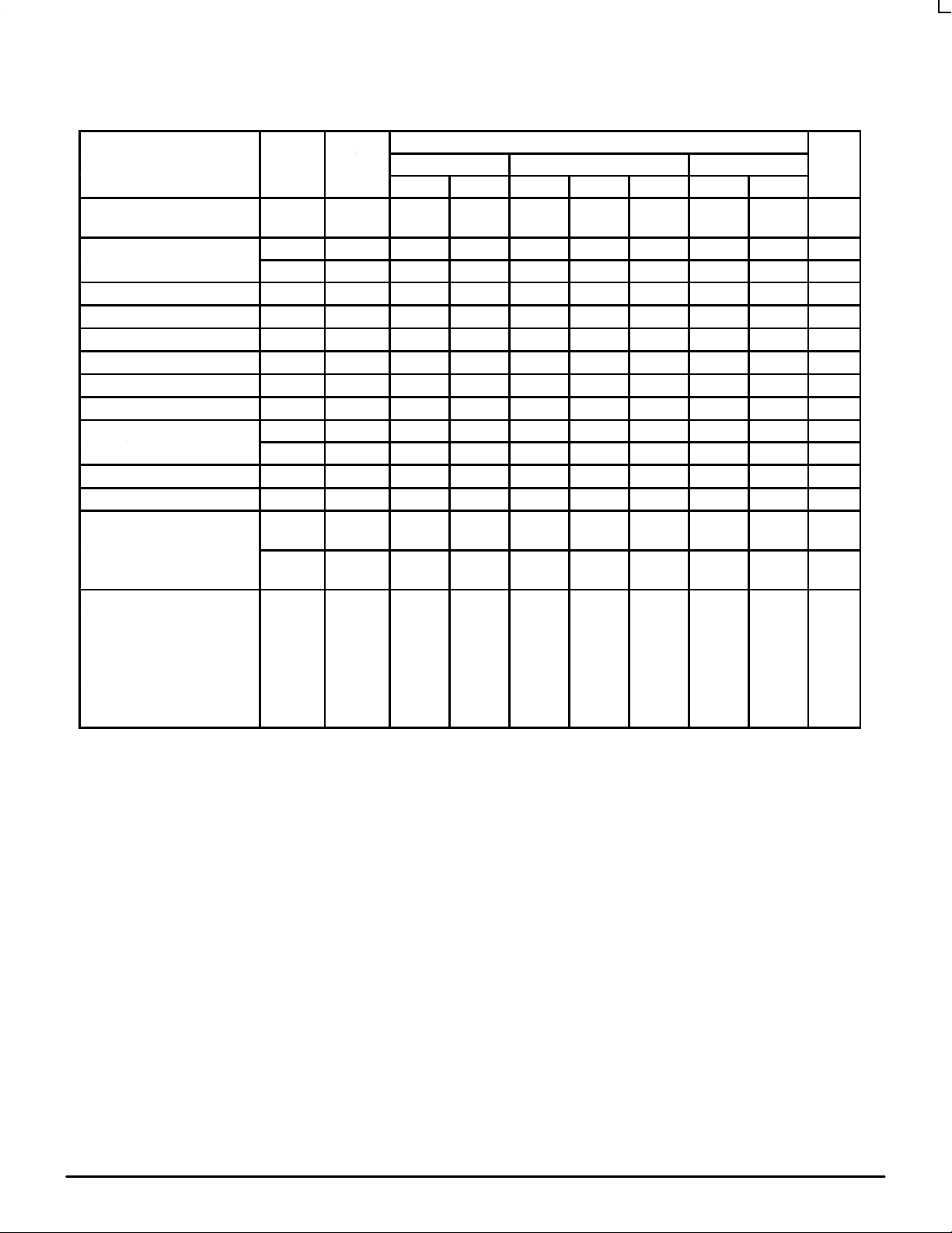
ELECTRICAL CHARACTERISTICS
Test Limits
Pin
Characteristic Symbol
Negative Power Supply Drain
Current
Positive Power Supply Drain
Current
Input Current I
Input Leakage Current I
High Output Voltage V
Low Output Voltage V
High Threshold Voltage V
Low Threshold Voltage V
Indeterminate Input
Protection Tests
Short Circuit Current I
Reference Voltage V
Common Mode Rejection
Tests
Switching Times (50Ω Load) ns
Propagation Delay
(50% to +1.5Vdc)
Rise Time (+1.0V to 2.0V) t
Fall Time (+1.0V to 2.0V) t
1. Individually test each output, apply V
I
CCH
I
CCL
inH
CBO
OHA
V
OLS1
V
OLS2
V
V
t
6+5–
t
6–5+
t
2+4–
t
2–4+
I
E
OH
OL
OLA
OS
BB
OH
OL
4+
4–
Under
Test
1
to pin under test.
IHmax
8 –44 –40 –44 mAdc
9 52 52 52 mAdc
9 39 39 39 mAdc
2 180 115 115 µAdc
2 1.5 1.0 1.0 µAdc
4 2.5 2.5 2.5 Vdc
4 0.5 0.5 0.5 Vdc
4 2.5 2.5 2.5 Vdc
4 0.5 0.5 0.5 Vdc
4 0.5 0.5 0.5 Vdc
4 0.5 0.5 0.5 Vdc
4 40 100 40 100 40 100 mAdc
1 –1.420 –1.280 –1.350 –1.230 –1.295 –1.150 Vdc
4
4
4
4
5
5
4
4
4 3.3 3.3 3.3
4 3.3 3.3 3.3
–30°C +25°C +85°C
Min Max Min Typ Max Min Max
2.5
2.5
1.0
1.0
1.0
1.0
0.5
0.5
6.0
6.0
6.0
6.0
2.5
2.5
1.0
1.0
1.0
1.0
4.5
4.5
4.5
4.5
0.5
0.5
6.0
6.0
6.0
6.0
2.5
2.5
1.0
1.0
1.0
1.0
0.5
0.5
6.0
6.0
6.0
6.0
Unit
Vdc
Vdc
MOTOROLA MECL Data
3–90
DL122 — Rev 6
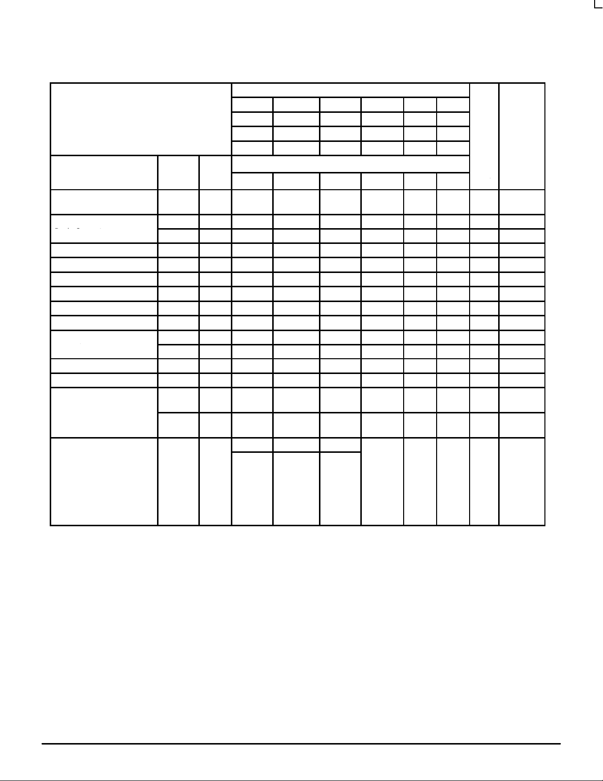
ELECTRICAL CHARACTERISTICS (continued)
Und
pp y
p
TEST VOLTAGE VALUES (Volts)
@ Test Temperature V
–30°C –0.890 –1.890 –1.205 –1.500 +0.110 –0.890
+25°C –0.810 –1.850 –1.105 –1.475 +0.190 –0.850
+85°C –0.700 –1.825 –1.035 –1.440 +0.300 –0.825
Pin
Characteristic Symbol
Negative Power Supply
Drain Current
Positive Power Supply
Drain Current
Input Current I
Input Leakage Current I
High Output Voltage V
Low Output Voltage V
High Threshold Voltage V
Low Threshold Voltage V
Indeterminate Input
Protection Tests
Short Circuit Current I
Reference Voltage V
Common Mode Rejection
Tests
Switching Times(50Ω Load) Pulse In Pulse Out CL (pF)
Propagation Delay
(50% to +1.5Vdc)
Rise Time (+1.0V to 2.0V) t
Fall Time (+1.0V to 2.0V) t
1. Individually test each output, apply V
I
CCH
I
CCL
inH
CBO
V
OLS1
V
OLS2
V
V
t
6+5–
t
6–5+
t
2+4–
t
2–4+
I
E
OH
OL
OHA
OLA
OS
BB
OH
OL
4+
4–
1
IHmax
Test
8 16
9 2,6,10,14 16
9 2,6,10,14
2 2,6,10,14 16
2 16
4 2,6,10,14 16 –2.0mA
4 2,6,10,14 16 20mA
4 6,10,14 2 16 –2.0mA
4 6,10,14 2 16 20mA
4 16 20mA
4 16 20mA
4 2,6,10,14 4, 16
1 2,6,10,14
4
4
4
4
5
5
4
4
4 2 4 25 16
4 2 4 25 16
to pin under test.
IHmax
er
V
IHmax
6
6
2
2
V
ILmin
TEST VOLTAGE APPLIED TO PINS LISTED BELOW
V
ILmin
5
5
4
4
V
IHAminVILAmaxVIHH
V
IHAminVILAmaxVIHH
25
25
25
25
V
ILH
ILH
Gnd
V
3 2 16
2 3 16
MC10125
Condition
16
16
16
16
16
16
16
Output
–2.0mA
–2.0mA
20mA
20mA
DL122 — Rev 6
3–91 MOTOROLAMECL Data
 Loading...