

MOTOROLA MC100EPT24DR2, MC100EPT24D Datasheet
MC100EPT24
LVTTL/LVCMOS to Differ ential
LVECL Translator
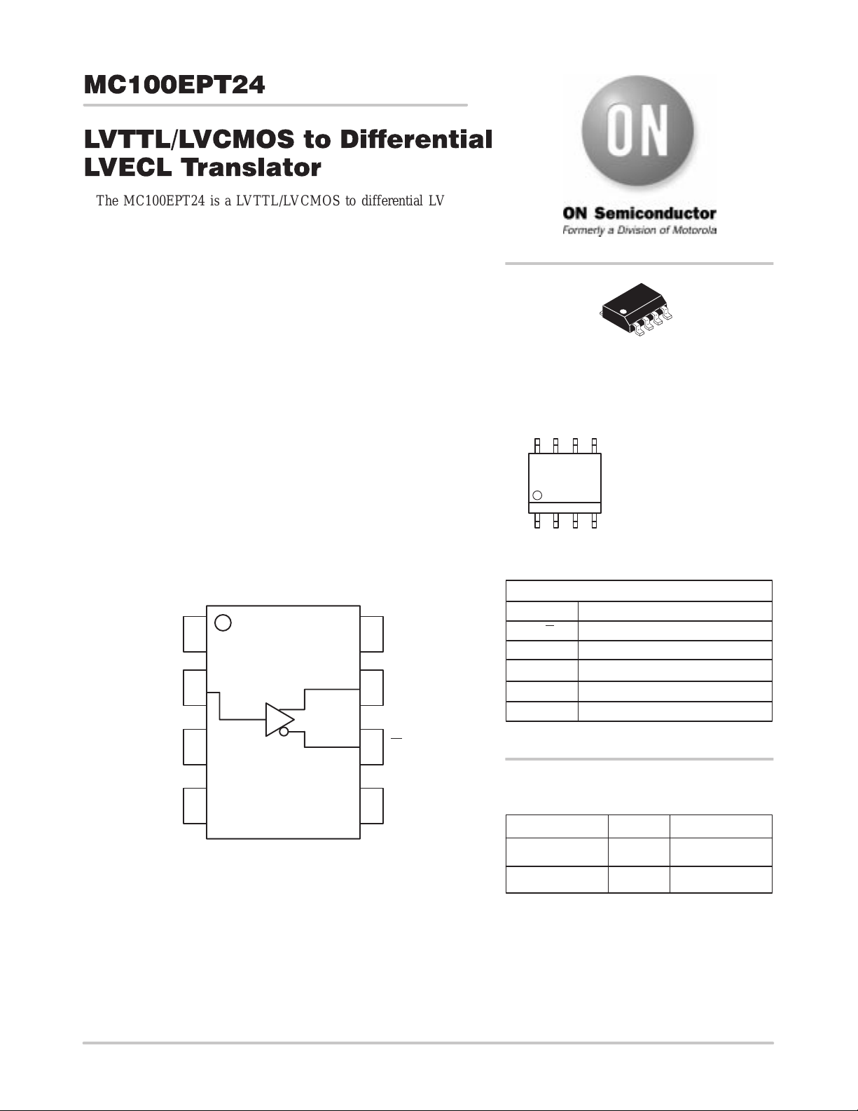
The MC100EPT24 is a LVTTL/LVCMOS to differential LVECL
translator. Because LVECL levels and LVTTL/LVCMOS levels are
used, a –3.3V, +3.3V and ground are required. The small outline
8–lead SOIC package and the single gate of the EPT24 makes it ideal
for those applications where space, performance, and low power are at
a premium.
The EPT24 is available in the 100E standard and is compatible with
ECL 100K logic levels.
http://onsemi.com
8
• 350ps T ypical Propagation Delay
• Maximum Frequency > 1.0GHz
• Differential ECL Outputs
• Small Outline SOIC Package
• PNP LVTTL Inputs for Minimal Loading
• Flow Through Pinouts
• Q Output will default HIGH with inputs open
• ESD Protection: 4000 KV HBM, 200 V MM
• Moisture Sensitivity Level 1, Indefinite Time Out of Drypack.
For Additional Information, See Application Note AND8003/D
• Flammability Rating: UL–94 code V–0 @ 1/8”,
Oxygen Index 28 to 34
• Transistor Count = 181 devices
V
EE
1
LVTTL
2
D
LVECL
3
78Q
6
V
CC
QNC
1
SO–8
D SUFFIX
CASE 751
MARKING DIAGRAM
8
KPT24
ALYW
1
*For additional information, see Application Note
AND8002/D
PIN DESCRIPTION
PIN
Q, Q
D LVTTL Input
V
CC
GND Ground
V
EE
A = Assembly Location
L = W afer Lot
Y = Year
W = Work Week
FUNCTION
Differential L VECL Outputs
Positive Supply
Negative Supply
45
NC
Figure 1. 8–Lead Pinout (Top View) and Logic Diagram
Semiconductor Components Industries, LLC, 1999
December, 1999 – Rev. 1
GND
MC100EPT24D SOIC 98 Units/Rail
MC100EPT24DR2 SOIC 2500 Tape & Reel
1 Publication Order Number:
ORDERING INFORMATION
Device Package Shipping
MC100EPT24/D

MC100EPT24
MAXIMUM RATINGS*
Symbol Parameter Value Unit
V
EE
V
CC
V
I
V
I
I
out
T
A
T
stg
θ
JA
θ
JC
T
sol
* Maximum Ratings are those values beyond which damage to the device may occur.
LVTTL INPUT DC CHARACTERISTICS (VCC = 3.3V ±0.3V; GND = 0V; TA = –40°C to +85°C)
Symbol Characteristic Min Typ Max Unit
I
IH
I
IHH
I
IL
V
V
V
IK
IH
IL
Input HIGH Current (Vin = 2.7V) 20 µA
Input HIGH Current MAX (Vin = 6.0V) 100 µA
Input LOW Current (Vin = 0.5V) –0.6 mA
Input Clamp Voltage (Iin = –18mA) –1.2 V
Input HIGH Voltage 2.0 V
Input LOW Voltage 0.8 V
Power Supply (VCC = 0V) –3.8 to 0 VDC
Power Supply (VEE = 0V) 3.8 to 0 VDC
Input Voltage (VCC = 0V, VI not more negative than VEE) –3.8 to 0 VDC
Input Voltage (VEE = 0V, VI not more positive than VCC) 3.8 to 0 VDC
Output Current Continuous
Surge
Operating Temperature Range –40 to +85 °C
Storage Temperature –65 to +150 °C
Thermal Resistance (Junction–to–Ambient) Still Air
500lfpm
Thermal Resistance (Junction–to–Case) 41 to 44 ± 5% °C/W
Solder Temperature (<2 to 3 Seconds: 245°C desired) 265 °C
50
100
190
130
mA
°C/W
LVECL OUTPUT DC CHARACTERISTICS (VCC = 3.3V ± 0.3V; VEE = –3.3V ± 0.3V; GND = 0V)
–40°C 25°C 85°C
Symbol Characteristic Min Typ Max Min Typ Max Min Typ Max Unit
V
OH
V
OL
I
CC
I
EE
1. Output levels will vary 1:1 with GND; Outputs loaded through 50W to GND – 2.0V.
Output HIGH Voltage (Note 1.) -1135 –1020 -885 -1135 –1020 -885 -1135 –1030 -885 mV
Output LOW Voltage (Note 1.) -1935 –1750 -1685 -1935 –1770 -1685 -1925 –1790 -1685 mV
Power Supply Current 2.0 4.0 2.0 4.0 2.0 4.0 mA
Power Supply Current 20 30 38 20 30 38 20 30 38 mA
AC CHARACTERISTICS (VCC = 3.3V ± 0.3V; VEE = –3.3V ± 0.3V; GND = 0V)
–40°C 25°C 85°C
Symbol Characteristic Min Typ Max Min Typ Max Min Typ Max Unit
f
max
t
PLH
t
PHL
t
JITTER
t
r
t
f
2. F
3. TTL input of 0V to 3V.
Maximum Toggle
Frequency (Note 2.)
,
Propagation Delay to
Output Differential (Note 3.)
Cycle–to–Cycle Jitter TBD TBD TBD ps
Output Rise/Fall Times Q, Q
(20% – 80%)
guaranteed for functionality only. VOL and VOH levels are guaranteed at DC only.
max
1.0 1.0 1.0 GHz
300 500 800 300 530 800 300 560 800 ps
70 125 170 80 130 180 100 150 200 ps
http://onsemi.com
2
 Loading...