

Motorola MC10E143FN, MC10E143FNR2, MC100E143FNR2, MC100E143FN Datasheet
D
2D3D4VCCOQ0Q1Q2
V
CCO
D
5
D
6
D
7
D
8
SEL
MR
CLK1
CLK2
V
EE
NC
D
0
D
1
26
27
28
2
3
4
25 24 23 22 21 20 19
18
17
16
15
14
13
12
115 6 7 8 9 10
Q
8
Q
7
Q
6
V
CC
Q
5
V
CCO
Q
4
Q
3
1
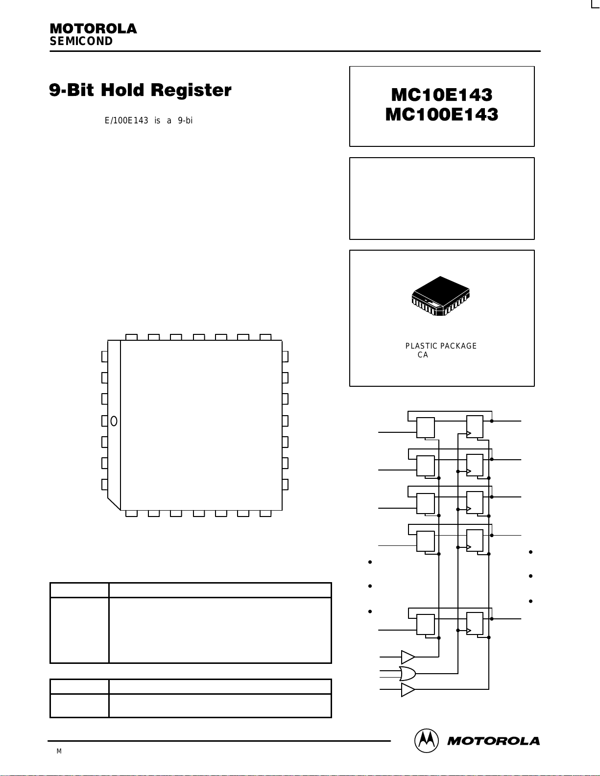
Pinout: 28-Lead PLCC (Top View)
* All VCC and V
CCO
pins are tied together on the die.
MUX
MUX
MUX
MUX
LOGIC DIAGRAM
D
0
D
1
D
2
D
3
D
8
SEL
CLK1
CLK2
MR
Q
0
Q
1
Q
2
Q
3
Q
8
MUX
D
R
D
D
D
D
R
R
R
R
SEMICONDUCTOR TECHNICAL DATA
2–1
REV 2
Motorola, Inc. 1996
12/93
The MC10E/100E143 is a 9-bit holding register, designed with
byte-parity applications in mind. The E143 holds current data or loads
new data, with the nine inputs D0 – D8 accepting parallel input data.
• 700MHz Min. Operating Frequency
• 9-Bit for Byte-Parity Applications
• Asynchronous Master Reset
• Dual Clocks
• Extended 100E V
EE
Range of – 4.2V to – 5.46V
• 75kΩ Input Pulldown Resistors
The SEL (Select) input pin is used to switch between the two modes of
operation — HOLD and LOAD. Input data is accepted by the registers a
set-up time before the positive going edge of CLK1 or CLK2. A HIGH on
the Master Reset pin (MR) asynchronously resets all the registers to zero.
PIN NAMES
Pin Function
D0 – D
8
Parallel Data Inputs
SEL Mode Select Input
CLK1, CLK2 Clock Inputs
MR Master Reset
Q0 – Q
8
Data Outputs
NC No Connection
FUNCTIONS
SEL Mode
L
H
Load
Hold
9-BIT HOLD
REGISTER
FN SUFFIX
PLASTIC PACKAGE
CASE 776-02
MC10E143 MC100E143
MOTOROLA ECLinPS and ECLinPS Lite
DL140 — Rev 4
2–2
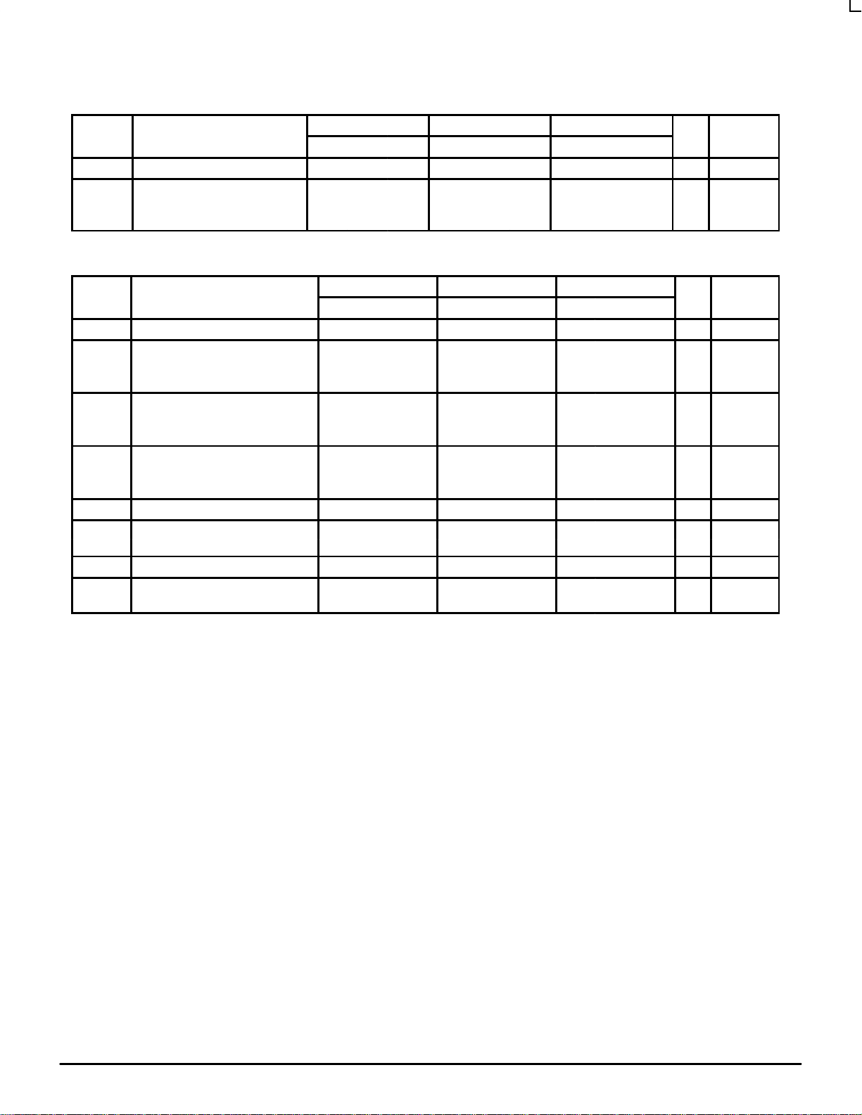
DC CHARACTERISTICS (VEE = VEE(min) to VEE(max); VCC = V
CCO
= GND)
0°C 25°C 85°C
Symbol Characteristic min typ max min typ max min typ max Unit Condition
I
IH
Input HIGH Current 150 150 150 µA
I
EE
Power Supply Current mA
10E 120 145 120 145 120 145
100E 120 145 120 145 138 165
AC CHARACTERISTICS (VEE = VEE(min) to VEE(max); VCC = V
CCO
= GND)
0°C 25°C 85°C
Symbol Characteristic min typ max min typ max min typ max Unit Condition
f
MAX
Max. Toggle Frequency 700 900 700 900 700 900 MHz
t
PLH
Propagation Delay to Output ps
t
PHL
Clk 600 800 1000 600 800 1000 600 800 1000
MR 600 800 1000 600 800 1000 600 800 1000
t
s
Setup Time ps
D 50 –100 50 –100 50 –100
SEL 300 150 300 150 300 150
t
h
Hold Time ps
D 300 100 300 100 300 100
SEL 75 –150 75 –150 75 –150
t
RR
Reset Recovery Time 900 700 900 700 900 700 ps
t
PW
Minimum Pulse Width ps
Clk, MR 400 400 400
t
SKEW
Within-Device Skew 75 75 75 ps 1
t
r
Rise/Fall Times ps
t
f
20 - 80% 300 525 800 300 525 800 300 525 800
1. Within-device skew is defined as identical transitions on similar paths through a device.
 Loading...