

Motorola MC10E137FN, MC10E137FNR2, MC100E137FN, MC100E137FNR2 Datasheet
SEMICONDUCTOR TECHNICAL DATA
2–1
REV 2
Motorola, Inc. 1996
7/96
The MC10E/100E137 is a very high speed binary ripple counter. The
two least significant bits were designed with very fast edge rates while the
more significant bits maintain standard ECLinPS output edge rates.
This allows the counter to operate at very high frequencies while
maintaining a moderate power dissipation level.
• 1.8GHz Minimum Count Frequency
• Differential Clock Input and Data Output Pins
• V
BB
Output for Single-Ended Use
• Internal 75kΩ Input Pulldown Resistors
• Synchronous and Asynchronous Enable Pins
• Asynchronous Master Reset
• Extended 100E V
EE
Range of –4.2V to –5.46V
The device is ideally suited for multiple frequency clock generation as
well as a counter in a high performance ATE time measurement board.
Both asynchronous and synchronous enables are available to
maximize the device’s flexibility for various applications. The
asynchronous enable input, A_Start, when asserted enables the counter
while overriding any synchronous enable signals. The E137 features
XORed enable inputs, EN1 and EN2, which are synchronous to the CLK
input. When only one synchronous enable is asserted the counter
becomes disabled on the next CLK transition; all outputs remain in the
previous state poised for the other synchronous enable or A_Start to be
asserted to re-enable the counter. Asserting both synchronous enables
causes the counter to become enabled on the next transition of the CLK.
If EN1 (or EN2) and CLK edges are coincident, sufficient delay has been
inserted in the CLK path (to compensate for the XOR gate delay and the
internal D-flip flop setup time) to insure that the synchronous enable
signal is clocked correctly, hence, the counter is disabled.
The E137 can also be driven single-endedly utilizing the VBB output
supply as the voltage reference for the CLK input signal. If a single-ended
signal is to be used the VBB pin should be connected to the CLK
input and
bypassed to ground via a 0.01µF capacitor. VBB can only source/sink
0.5mA, therefore it should be used as a switching reference for the E137
only.
All input pins left open will be pulled LOW via an input pulldown resistor. Therefore, do not leave the differential CLK inputs
open. Doing so causes the current source transistor of the input clock gate to become saturated, thus upsetting the internal bias
regulators and jeopardizing the stability of the device.
The asynchronous Master Reset resets the counter to an all zero state upon assertion.
CLK
CLK
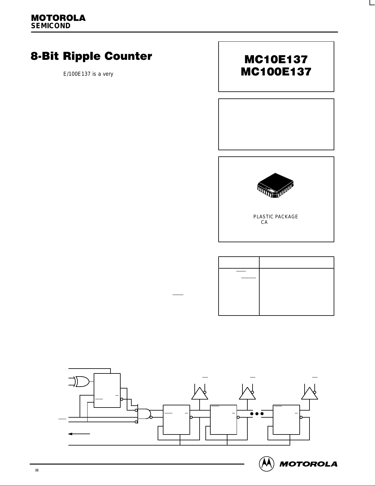
LOGIC DIAGRAM
Q
Q
CLK
CLK
D
R
Q
Q
CLK
CLK
D
R
EN1
EN2
CLK
CLK
A_Start
Q
Q
D
R
Q0 Q0 Q1 Q1
Q
Q
CLK
CLK
D
R
Q7 Q7
MR
V
BB
8-BIT RIPPLE
COUNTER
FN SUFFIX
PLASTIC PACKAGE
CASE 776-02
CLK, CLK
Q0-Q7, Q0-Q7
A_Start
EN1, EN2
MR
V
BB
Differential Clock Inputs
Differential Q Outputs
Asynchronous Enable Input
Synchronous Enable Inputs
Asynchronous Master Reset
Switching Refernce Output
PIN FUNCTION
PIN NAMES

MC10E137 MC100E137
MOTOROLA ECLinPS and ECLinPS Lite
DL140 — Rev 4
2–2
V
CCO
1
Q0
Q7 Q7 Q6 Q6 Q5 Q5
Q4
Q4
V
CC
Q3
Q3
Q2
Q2
V
CCO
Q1Q1Q0
V
CCO
MR
V
BB
CLK
CLK
V
EE
EN2
EN1
A_Start
4
3
2
28
27
26
25
24
23
22
21
20
19
18
17
16
15
14
13
12
11109
7
8
6
5
Pinout: 28-Lead PLCC (Top View)
* All VCC and V
CCO
pins are tied together on the die.
SEQUENTIAL TRUTH TABLE
Function EN1 EN2 A_Start MR CLK Q7 Q6 Q5 Q4 Q3 Q2 Q1 Q0
Reset X X X H X L L L L L L L L
Count L
L
L
L
L
L
L
L
L
L
L
L
Z
Z
Z
L
L
L
L
L
L
L
L
L
L
L
L
L
L
L
L
L
L
L
H
H
H
L
H
Stop H
H
L
L
L
L
L
L
Z
Z
L
L
L
L
L
L
L
L
L
L
L
L
H
H
H
H
Asynch Start H
H
L
L
L
L
H
H
H
L
L
L
Z
Z
Z
L
L
L
L
L
L
L
L
L
L
L
L
L
L
L
H
H
H
L
L
H
L
H
L
Count L
L
L
L
L
L
L
L
L
L
L
L
Z
Z
Z
L
L
L
L
L
L
L
L
L
L
L
L
L
H
H
H
L
L
H
L
L
H
L
H
Stop L
L
H
H
L
L
L
L
Z
Z
L
L
L
L
L
L
L
L
H
H
L
L
L
L
H
H
Synch Start H
H
H
H
H
H
L
L
L
L
L
L
Z
Z
Z
L
L
L
L
L
L
L
L
L
L
L
L
H
H
H
L
L
H
H
H
L
L
H
L
Stop H
H
L
L
L
L
L
L
Z
Z
L
L
L
L
L
L
L
L
H
H
H
H
L
L
L
L
Count L
L
L
L
L
L
L
L
L
L
L
L
Z
Z
Z
L
L
L
L
L
L
L
L
L
L
L
L
H
H
H
H
H
H
L
H
H
H
L
H
Reset X X X H X L L L L L L L L
Z = Low to High Transition
 Loading...