

查询MC100E111FN供应商
SEMICONDUCTOR TECHNICAL DATA
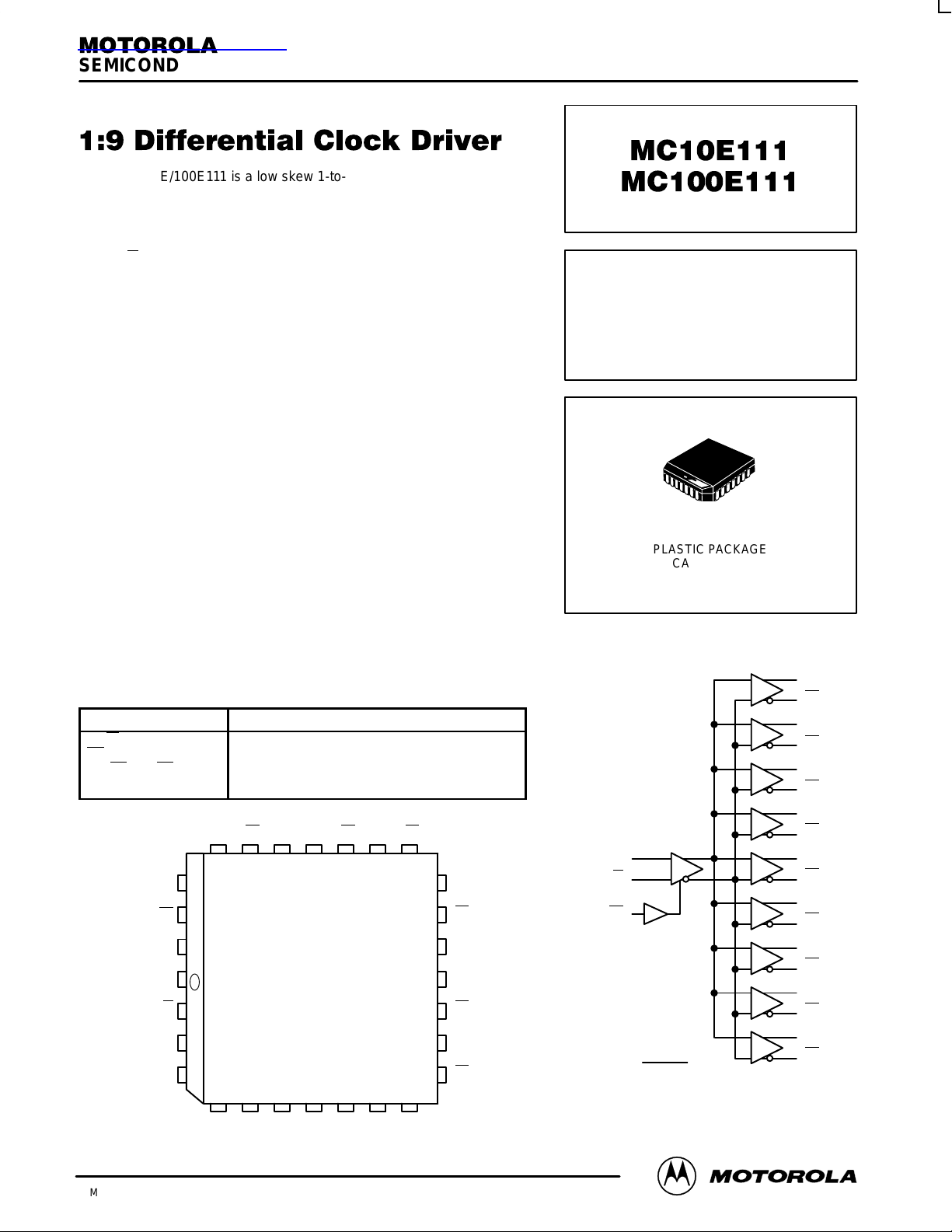
The MC10E/100E111 is a low skew 1-to-9 differential driver, designed
with clock distribution in mind. It accepts one signal input, which can be
either differential or else single-ended if the VBB output is used. The
signal is fanned out to 9 identical differential outputs. An enable input is
also provided. A HIGH disables the device by forcing all Q outputs LOW
and all Q
• Low Skew
• Guarateed Skew Spec
• Differential Design
• V
• Enable
• Extended 100E V
• 75kΩ Input Pulldown Resistors
skew as the key goal. Optimal design and layout serve to minimize gate to
gate skew within-device, and empirical modeling is used to determine
process control limits that ensure consistent tpd distributions from lot to
lot. The net result is a dependable, guaranteed low skew device.
both sides of the differential output are terminated into 50Ω, even if only
one side is being used. In most applications, all nine differential pairs will
be used and therefore terminated. In the case where fewer than nine
pairs are used, it is necessary to terminate at least the output pairs on the
same package side (i.e. sharing the same V
used on that side, in order to maintain minimum skew. Failure to do this
will result in small degradations of propagation delay (on the order of
10–20ps) of the output(s) being used which, while not being catastrophic
to most designs, will mean a loss of skew margin.
PIN NAMES
IN, IN
EN
Q0, Q0–Q8, Q
V
outputs HIGH.
Output
BB
Range of –4.2 to –5.46V
EE
The device is specifically designed, modeled and produced with low
To ensure that the tight skew specification is met it is necessary that
) as the pair(s) being
CCO
Pin Function
Differential Input Pair
Enable
Differential Outputs
VBB Output
Q0Q0Q1V
25 24 23 22 21 20 19
1
Pinout: 28-Lead PLCC
567891011
CCOQ1Q2Q2
(Top View)
18
17
16
15
14
13
12
Q
3
Q
3
Q
4
V
CCO
Q
4
Q
5
Q
5
BB
8
V
26
EE
27
EN
28
IN
V
CC
2
IN
3
V
BB
NC
4
1:9 DIFFERENTIAL
CLOCK DRIVER
FN SUFFIX
PLASTIC PACKAGE
CASE 776-02
LOGIC SYMBOL
IN
IN
EN
V
BB
Q
0
Q
0
Q
1
Q
1
Q
2
Q
2
Q
3
Q
3
Q
4
Q
4
Q
5
Q
5
Q
6
Q
6
Q
7
Q
7
Q
8
Q
8
5/95
Motorola, Inc. 1996
Q
8
Q
Q
8
7
V
CCOQ7
2–1
Q
Q
6
6
REV 3
MC10E111 MC100E111
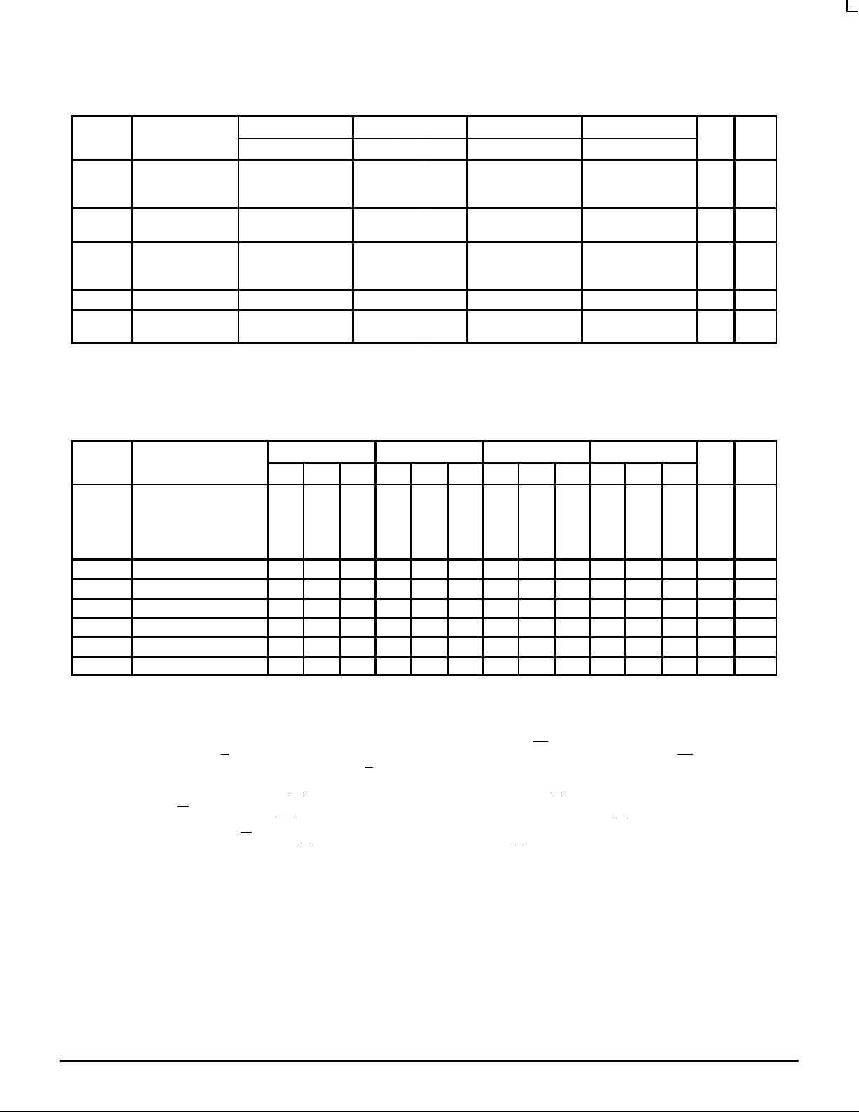
DC CHARACTERISTICS (VEE = VEE (min) to VEE (max); VCC = V
–40°C 0°C 25°C 85°C
Symbol Characteristic Min Typ Max Min Typ Max Min Typ Max Min Typ Max Unit Cond
V
BB
I
IH
I
EE
VPP(DC) Input Sensitivity 50 50 50 50 mV 1
V
CMR
1. Differential input voltage required to obtain a full ECL swing on the outputs.
2. V
CMR
must be such that the peak to peak voltage is less than 1.0 V and greater than or equal to VPP(min).
Output Reference
Voltage 10E
Input HIGH
Current
Power Supply
Current 10E
Commom Mode
Range
is defined as the range within which the VIH level may vary, with the device still meeting the propagation delay specification. The VIL level
–1.43
100E
–1.38
100E
–1.6 –0.4 –1.6 –0.4 –1.6 –0.4 –1.6 –0.4 V 2
–1.30
–1.38
–1.26
–1.38
150 150 150 150 µA
484860
60
–1.27
–1.26
484860
AC CHARACTERISTICS (VEE = VEE (min) to VEE (max); VCC = V
–40°C 0°C 25°C 85°C
Symbol Characteristic Min Typ Max Min Typ Max Min Typ Max Min Typ Max Unit Cond
t
PLH
t
PHL
t
s
t
H
t
R
t
skew
VPP(AC) Minimum Input Swing 250 250 250 250 mV 8
tr, t
f
1. The differential propagation delay is defined as the delay from the crossing points of the differential input signals to the crossing point of the
differential output signals. See
ECL Data Book (DL140/D).
2. The single-ended propagation delay is defined as the delay from the 50% point of the input signal to the 50% point of the output signal. See
Definitions and T esting of ECLinPS AC Parameters
3. Enable is defined as the propagation delay from the 50% point of a negative transition on EN
(or a negative transition on Q
of a negative transition on Q (or a positive transition on Q
4. The within-device skew is defined as the worst case difference between any two similar delay paths within a single device.
5. The setup time is the minimum time that EN
±75 mV to that IN/IN
6. The hold time is the minimum time that EN
greater than ±75 mV to that IN/IN
7. The release time is the minimum time that EN
the specified IN to Q propagation delay and output transition times (see Figure 3).
8. VPP(min) is defined as the minimum input differential voltage which will cause no increase in the propagation delay . The VPP(min) is AC limited
for the E111 as a differential input as low as 50 mV will still produce full ECL levels at the output.
Propagation Delay to
Output IN (Diff)
IN (SE)
Enable
Disable
Setup Time EN to IN 250 0 200 0 200 0 200 0 ps 5
Hold Time IN to EN 50 –200 0 –200 0 –200 0 –200 ps 6
Release Time EN to IN 350 100 300 100 300 100 300 100 ps 7
Within-Device Skew 25 75 25 50 25 50 25 50 ps 4
Rise/Fall Time 250 450 650 275 375 600 275 375 600 275 375 600 ps
380
280
400
400
680
780
900
900
460
410
450
450
Definitions and T esting of ECLinPS AC Parameters
in Chapter 1 (page 1–12) of the Motorola High Performance ECL Data Book (DL140/D).
). Disable is defined as the propagation delay from the 50% point of a positive transition on EN to the 50% point
must be asserted prior to the next transition of IN/IN to prevent an output response greater than
transition (see Figure 1).
must remain asserted after a negative going IN or a positive going IN to prevent an output response
transition (see Figure 2).
must be deasserted prior to the next IN/IN transition to ensure an output response that meets
).
60
= GND)
CCO
–1.35
–1.38
= GND)
CCO
560
480
610
430
850
450
850
450
in Chapter 1 (page 1–12) of the Motorola High Performance
–1.25
–1.31
–1.26
–1.38
484860
60
580
510
630
460
850
450
850
450
to the 50% point of a positive transition on Q
–1.19
–1.26
485560
69
610
660
850
850
V
mA
ps
1
2
3
3
MOTOROLA ECLinPS and ECLinPS Lite
2–2
DL140 — Rev 4

MC10E111 MC100E111
IN
IN
t
s
EN
Q
Q
50%
Figure 1. Setup Time
IN
IN
EN
Q
Q
t
h
50%
Figure 2. Hold Time
≤
75mV
≤
75mV
≤
75mV
≤
75mV
IN
IN
EN
Q
Q
t
r
50%
Figure 3. Release Time
DL140 — Rev 4
2–3 MOTOROLAECLinPS and ECLinPS Lite

MC10E111 MC100E111
-N-
-L-
28 1
OUTLINE DIMENSIONS
FN SUFFIX
PLASTIC PLCC PACKAGE
CASE 776–02
ISSUE D
SNSM
G1
–M
SNSM
–M
0.010 (0.250) T L
–M
SNSS
0.007 (0.180) T L
Y BRK
B
0.007 (0.180) T L
U
D
Z
-M-
D
W
V
X
VIEW D-D
Z
C
G
G1
0.010 (0.250) T L
0.007 (0.180) T L
A
0.007 (0.180) T L
R
E
0.004 (0.100)
SEATING
-T-
J
PLANE
VIEW S
SNSS
–M
NOTES:
1. DATUMS -L-, -M-, AND -N- DETERMINED
WHERE TOP OF LEAD SHOULDER EXITS
PLASTIC BODY AT MOLD PARTING LINE.
2. DIM G1, TRUE POSITION TO BE MEASURED
AT DATUM -T-, SEATING PLANE.
3. DIM R AND U DO NOT INCLUDE MOLD FLASH.
ALLOWABLE MOLD FLASH IS 0.010 (0.250)
PER SIDE.
4. DIMENSIONING AND TOLERANCING PER ANSI
Y14.5M, 1982.
5. CONTROLLING DIMENSION: INCH.
6. THE PACKAGE TOP MAY BE SMALLER THAN
THE PACKAGE BOTTOM BY UP TO 0.012
(0.300). DIMENSIONS R AND U ARE
DETERMINED AT THE OUTERMOST
EXTREMES OF THE PLASTIC BODY
EXCLUSIVE OF MOLD FLASH, TIE BAR
BURRS, GATE BURRS AND INTERLEAD
FLASH, BUT INCLUDING ANY MISMATCH
BETWEEN THE TOP AND BOTTOM OF THE
PLASTIC BODY.
7. DIMENSION H DOES NOT INCLUDE DAMBAR
PROTRUSION OR INTRUSION. THE DAMBAR
PROTRUSION(S) SHALL NOT CAUSE THE H
DIMENSION TO BE GREATER THAN 0.037
(0.940). THE DAMBAR INTRUSION(S) SHALL
NOT CAUSE THE H DIMENSION TO BE
SMALLER THAN 0.025 (0.635).
–M
–M
SNSM
SNSM
H
0.007 (0.180) T L
–M
SNSM
K1
K
SNSM
0.007 (0.180) T L
F
–M
VIEW S
INCHES MILLIMETERS
MIN MINMAX MAX
DIM
A
B
C
G
H
K
R
U
W
G1
K1
E
F
J
V
X
Y
Z
0.485
0.485
0.165
0.090
0.013
0.050 BSC
0.026
0.020
0.025
0.450
0.450
0.042
0.042
0.042
—
°
2
0.410
0.040
0.495
0.495
0.180
0.110
0.019
0.032
—
—
0.456
0.456
0.048
0.048
0.056
0.020
10
0.430
—
12.32
12.57
12.32
12.57
4.20
4.57
2.29
2.79
0.33
0.48
1.27 BSC
0.66
0.81
0.51
—
0.64
—
11.43
11.58
11.43
11.58
1.07
1.21
1.07
1.21
1.07
1.42
—
0.50
°
°
2
1.02
10
10.92
—
°
10.42
MOTOROLA ECLinPS and ECLinPS Lite
2–4
DL140 — Rev 4

MC10E111 MC100E111
Motorola reserves the right to make changes without further notice to any products herein. Motorola makes no warranty , representation or guarantee regarding
the suitability of its products for any particular purpose, nor does Motorola assume any liability arising out of the application or use of any product or circuit, and
specifically disclaims any and all liability, including without limitation consequential or incidental damages. “T ypical” parameters which may be provided in Motorola
data sheets and/or specifications can and do vary in different applications and actual performance may vary over time. All operating parameters, including “Typicals”
must be validated for each customer application by customer’s technical experts. Motorola does not convey any license under its patent rights nor the rights of
others. Motorola products are not designed, intended, or authorized for use as components in systems intended for surgical implant into the body, or other
applications intended to support or sustain life, or for any other application in which the failure of the Motorola product could create a situation where personal injury
or death may occur. Should Buyer purchase or use Motorola products for any such unintended or unauthorized application, Buyer shall indemnify and hold Motorola
and its officers, employees, subsidiaries, affiliates, and distributors harmless against all claims, costs, damages, and expenses, and reasonable attorney fees
arising out of, directly or indirectly, any claim of personal injury or death associated with such unintended or unauthorized use, even if such claim alleges that
Motorola was negligent regarding the design or manufacture of the part. Motorola and are registered trademarks of Motorola, Inc. Motorola, Inc. is an Equal
Opportunity/Affirmative Action Employer.
How to reach us:
USA/EUROPE /Locations Not Listed: Motorola Literature Distribution; JAPAN: Nippon Motorola Ltd.; Tatsumi–SPD–JLDC, 6F Seibu–Butsuryu–Center,
P.O. Box 20912; Phoenix, Arizona 85036. 1–800–441–2447 or 602–303–5454 3–14–2 Tatsumi Koto–Ku, Tokyo 135, Japan. 03–81–3521–8315
MFAX: RMF AX0@email.sps.mot.com – T OUCHTONE 602–244–6609 ASIA/P ACIFIC: Motorola Semiconductors H.K. Ltd.; 8B Tai Ping Industrial Park,
INTERNET: http://Design–NET .com 51 Ting Kok Road, Tai Po, N.T., Hong Kong. 852–26629298
MC10E111/D
DL140 — Rev 4
◊
2–5 MOTOROLAECLinPS and ECLinPS Lite
*MC10E111/D*
 Loading...