


SEMICONDUCTOR TECHNICAL DATA
2–1
REV 2
Motorola, Inc. 1996
12/93
The MC10E/100E016 is a high-speed synchronous, presettable,
cascadable 8-bit binary counter. Architecture and operation are the same
as the MC10H016 in the MECL 10H family , extended to 8-bits, as shown
in the logic symbol.
The counter features internal feedback of TC
, gated by the TCLD
(terminal count load) pin. When TCLD is LOW (or left open, in which case
it is pulled LOW by the internal pull-downs), the TC
feedback is disabled,
and counting proceeds continuously, with TC
going LOW to indicate an
all-one state. When TCLD is HIGH, the TC
feedback causes the counter
to automatically reload upon TC
= LOW, thus functioning as a
programmable counter. The Qn outputs do not need to be terminated for
the count function to operate properly. To minimize noise and power,
unused Q outputs should be left unterminated.
• 700MHz Min. Count Frequency
• 1000ps CLK to Q, TC
• Internal TC Feedback (Gated)
• 8-Bit
• Fully Synchronous Counting and TC Generation
• Asynchronous Master Reset
• Extended 100E V
EE
Range of – 4.2V to – 5.46V
• 75kΩ Input Pulldown Resistors
FUNCTION TABLE
CE PE TCLD MR CLK Function
X L X L Z Load Parallel (Pn to Qn)
L H L L Z Continuous Count
L H H L Z Count; Load Parallel on TC = LOW
H H X L Z Hold
X X X L ZZ Masters Respond, Slaves Hold
X X X H X Reset (Qn : = LOW, TC : = HIGH)
Z = clock pulse (low to high);
ZZ = clock pulse (high to low)
PIN NAMES
Pin Function
P0 – P
7
Parallel Data (Preset) Inputs
Q0– Q
7
Data Outputs
CE Count Enable Control Input
PE Parallel Load Enable Control Input
MR Master Reset
CLK Clock
TC Terminal Count Output
TCLD TC-Load Control Input
8-BIT SYNCHRONOUS
BINARY UP COUNTER
FN SUFFIX
PLASTIC PACKAGE
CASE 776-02
1
Pinout: 28-Lead PLCC (Top View)
MR
CLK
TCLD
V
EE
NC
P
0
P
1
26
27
28
2
3
4
25 24 23 22 21 20 19
18
17
16
15
14
13
12
115 6 7 8 9 10
PE
CE P7P6P5V
CCO
TC
Q
7
Q
6
V
CC
Q
5
Q
4
Q
3
P2P3P4V
CCOQ0Q1Q2
V
CCO
* All VCC and V
CCO
pins are tied together on the die.
查询MC100E016供应商

MC10E016 MC100E016
MOTOROLA ECLinPS and ECLinPS Lite
DL140 — Rev 4
2–2
8-BIT BINARY COUNTER LOGIC DIAGRAM
Note that this diagram is provided for understanding of logic operation only.
It should not be used for propagation delays as many gate functions are achieved internally without incurring a full gate delay.
P
1
SLAVEMASTER
5
TC
Q
1
Q
0
P7
Q
6
Q
5
Q
4
Q
3
Q
2
Q
1
CE
Q
0
BIT 1
CE
Q
0
Q0M
Q0M
BIT 0
PE
TCLD
CE
PO
MR
CLK
BIT 7
BITS 2–6
Q
7

MC10E016 MC100E016
2–3 MOTOROLAECLinPS and ECLinPS Lite
DL140 — Rev 4
DC CHARACTERISTICS (VEE = VEE(min) to VEE(max); VCC = V
CCO
= GND)
0°C 25°C 85°C
Symbol Characteristic min typ max min typ max min typ max Unit Condition
I
IH
Input HIGH Current 150 150 150 µA
I
EE
Power Supply Current mA
10E 151 181 151 181 151 181
100E 151 181 151 181 174 208
AC CHARACTERISTICS (VEE = VEE(min) to VEE(max); VCC = V
CCO
= GND)
0°C 25°C 85°C
Symbol Characteristic min typ max min typ max min typ max Unit Condition
f
COUNT
Max. Count Frequency 700 900 700 900 700 900 MHz
t
PLH
Propagation Delay to Output ps
t
PHL
CLK to Q 600 725 1000 600 725 1000 600 725 1000
MR to Q 600 775 1000 600 775 1000 600 775 1000
CLK to TC 550 775 900 550 775 900 550 775 1050
MR to TC 625 775 1000 625 775 1000 625 775 1000
t
s
Setup Time ps
Pn 150 – 30 150 – 30 150 – 30
CE 600 400 600 400 600 400
PE 600 400 600 400 600 400
TCLD 500 300 500 300 500 300
t
h
Hold Time
Pn 350 100 350 100 350 100
CE 0 – 400 0 – 400 0 – 400
PE 0 – 400 0 – 400 0 – 400
TCLD 100 – 300 100 – 300 100 – 300
t
RR
Reset Recovery Time 900 700 900 700 900 700 ps
t
PW
Minimum Pulse Width ps
CLK, MR 400 400 400
t
r
Rise/Fall Times ps
t
f
20 - 80% 300 510 800 300 510 800 300 510
MC10E016 MC100E016
MOTOROLA ECLinPS and ECLinPS Lite
DL140 — Rev 4
2–4
FUNCTION TABLE
Function PE CE MR TCLD CLK P7-P4 P3 P2 P1 P0 Q7-Q4 Q3 Q2 Q1 Q0 TC
Load L X L X Z H H H L L H H H L L H
Count H L L L Z X X X X X H H H L H H
H L L L Z X X X X X H H H H L H
H L L L Z X X X X X H H H H H L
H L L L Z X X X X X L L L L L H
Load L X L X Z H H H L L H H H L L H
Hold H H L X Z X X X X X H H H L L H
H H L X Z X X X X X H H H L L H
Load On H L L H Z H L H H L H H H L H H
Terminal H L L H Z H L H H L H H H H L H
Count H L L H Z H L H H L H H H H H L
H L L H Z H L H H L H L H H L H
H L L H Z H L H H L H L H H H H
H L L H Z H L H H L H H L L L H
Reset X X H X X X X X X X L L L L L H
Applications Information
Cascading Multiple E016 Devices
For applications which call for larger than 8-bit counters
multiple E016s can be tied together to achieve very wide
bit width counters. The active low terminal count (TC)
output and count enable input (CE
) greatly facilitate the
cascading of E016 devices. Two E016s can be cascaded
without the need for external gating, however for counters
wider than 16 bits external OR gates are necessary for
cascade implementations.
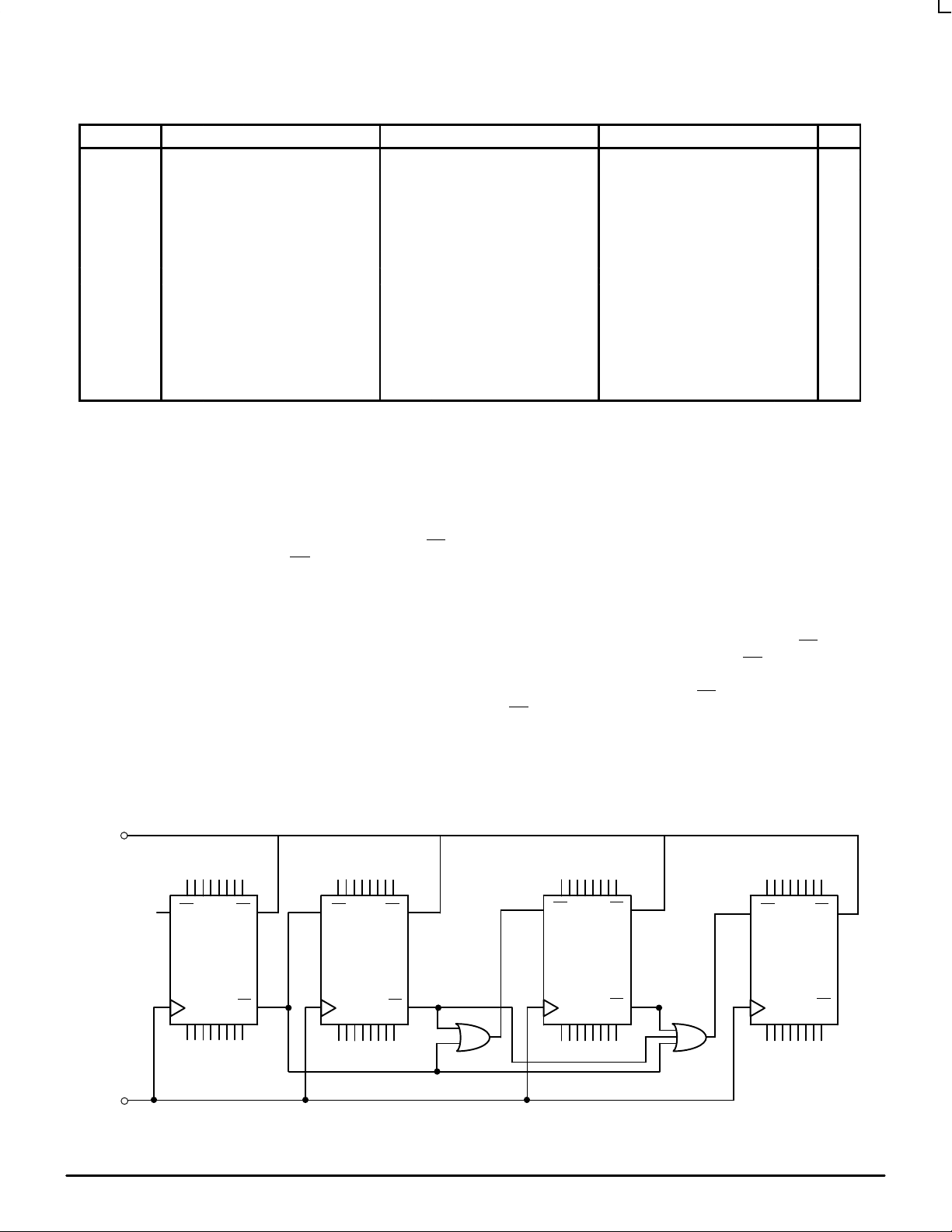
Figure 1 below pictorially illustrates the cascading of 4
E016s to build a 32-bit high frequency counter. Note the E101
gates used to OR the terminal count outputs of the lower order
E016s to control the counting operation of the higher order
bits. When the terminal count of the preceding device (or
devices) goes low (the counter reaches an all 1s state) the
more significant E016 is set in its count mode and will count
one binary digit upon the next positive clock transition. In
addition, the preceding devices will also count one bit thus
sending their terminal count outputs back to a high state
disabling the count operation of the more significant counters
and placing them back into hold modes. Therefore, for an
E016 in the chain to count, all of the lower order terminal count
outputs must be in the low state. The bit width of the counter
can be increased or decreased by simply adding or
subtracting E016 devices from Figure 1 and maintaining the
logic pattern illustrated in the same figure.
The maximum frequency of operation for the cascaded
counter chain is set by the propagation delay of the TC
output
and the necessary setup time of the CE
input and the
propagation delay through the OR gate controlling it (for 16-bit
counters the limitation is only the TC propagation delay and
the CE
setup time). Figure 1 shows EL01 gates used to control
the count enable inputs, however, if the frequency of operation
is lower a slower , ECL OR gate can be used. Using the worst
case guarantees for these parameters from the ECLinPS data
book, the maximum count frequency for a greater than 16-bit
counter is 500MHz and that for a 16-bit counter is 625MHz.
Figure 1. 32-Bit Cascaded E016 Counter
EL01
CLOCK
P0 –> P7
TC
CLK
P0 –> P7
TCCLK
EL01
P0 –> P7
TC
CLK
P0 –> P7
MSB
E016
PE
CE
Q0 –> Q7Q0 –> Q7 Q0 –> Q7
E016
PE
CE
Q0 –> Q7
E016
PE
CE
LSB
E016
PECE
LO
LOAD
TCCLK
MC10E016 MC100E016
2–5 MOTOROLAECLinPS and ECLinPS Lite
DL140 — Rev 4
Applications Information (continued)
Note that this assumes the trace delay between the TC
outputs and the CE inputs are negligible. If this is not
the case estimates of these delays need to be added to
the calculations.
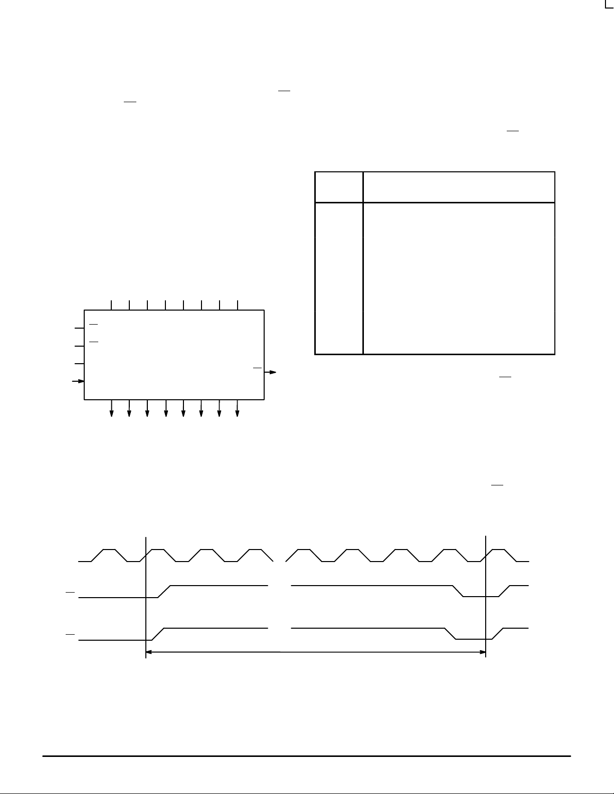
Programmable Divider
The E016 has been designed with a control pin which
makes it ideal for use as an 8-bit programmable divider. The
TCLD pin (load on terminal count) when asserted reloads the
data present at the parallel input pin (Pn’s) upon reaching
terminal count (an all 1s state on the outputs). Because this
feedback is built internal to the chip, the programmable
division operation will run at very nearly the same frequency
as the maximum counting frequency of the device. Figure 2
below illustrates the input conditions necessary for utilizing the
E016 as a programmable divider set up to divide by 113.
H
L
H
H L L L H H H H
TC
PE
CE
TCLD
CLK
P7 P6 P4 P3 P2 P1 P0P5
Q7 Q6 Q4 Q3 Q2 Q1 Q0Q5
Figure 2. Mod 2 to 256 Programmable Divider
To determine what value to load into the device to
accomplish the desired division, the designer simply subtracts
the binary equivalent of the desired divide ratio from the binary
value for 256. As an example for a divide ratio of 113:
Pn’s = 256 – 113 = 8F16 = 1000 1111
where:
P0 = LSB and P7 = MSB
Forcing this input condition as per the setup in Figure 2 will
result in the waveforms of Figure 3. Note that the TC
output is
used as the divide output and the pulse duration is equal to a
Table 1. Preset Values for Various Divide Ratios
Divide
Preset Data Inputs
P7 P6 P5 P4 P3 P2 P1 P0
2 H H H H H H H L
3 H H H H H H L H
4 H H H H H H L L
5 H H H H H L H H
• • • • • • • • •
• • • • • • • • •
112 H L L H L L L L
113 H L L L H H H H
114 H L L L H H H L
• • • • • • • • •
• • • • • • • • •
254 L L L L L L H L
255 L L L L L L L H
256 L L L L L L L L
full clock period. For even divide ratios, twice the desired
divide ratio can be loaded into the E016 and the TC
output can
feed the clock input of a toggle flip flop to create a signal
divided as desired with a 50% duty cycle.
A single E016 can be used to divide by any ratio from 2 to
256 inclusive. If divide ratios of greater than 256 are needed
multiple E016s can be cascaded in a manner similar to that
already discussed. When E016s are cascaded to build larger
dividers the TCLD pin will no longer provide a means for
loading on terminal count. Because one does not want to
reload the counters until all of the devices in the chain have
reached terminal count, external gating of the TC pins must be
used for multiple E016 divider chains.
•••
PE
•••
•••
Clock
TC
Load
DIVIDE BY 113
Load1001 0000 1001 0001 1111 1100 1111 1101 1111 1110 1111 1111
Figure 3. Divide by 113 E016 Programmable Divider Waveforms
Ratio
MC10E016 MC100E016
MOTOROLA ECLinPS and ECLinPS Lite
DL140 — Rev 4
2–6
Applications Information (continued)
E016
MSB
CLK TC
PECE
E016
CLK TC
PECE
E016
CLK TC
PECE
EL01
EL01
EL01
CLOCK
Q0 –> Q7
PO –> P7
Q0 –> Q7
PO –> P7
Q0 –> Q7
PO –> P7
Q0 –> Q7
PO –> P7
LO
E016
LSB
CLK TC
PECE
Figure 4. 32-Bit Cascaded E016 Programmable Divider
Figure 4 on the following page shows a typical block
diagram of a 32-bit divider chain. Once again to maximize the
frequency of operation EL01 OR gates were used. For lower
frequency applications a slower OR gate could replace the
EL01. Note that for a 16-bit divider the OR function feeding the
PE
(program enable) input CANNOT be replaced by a wire OR
tie as the TC
output of the least significant E016 must also feed
the CE
input of the most significant E016. If the two TC outputs
were OR tied the cascaded count operation would not operate
properly. Because in the cascaded form the PE feedback is
external and requires external gating, the maximum frequency
of operation will be significantly less than the same operation
in a single device.
Maximizing E016 Count Frequency
The E016 device produces 9 fast transitioning single ended
outputs, thus VCC noise can become significant in situations
where all of the outputs switch simultaneously in the same
direction. This VCC noise can negatively impact the maximum
frequency of operation of the device. Since the device does
not need to have the Q outputs terminated to count properly,
it is recommended that if the outputs are not going to be used
in the rest of the system they should be left unterminated. In
addition, if only a subset of the Q outputs are used in the
system only those outputs should be terminated. Not
terminating the unused outputs will not only cut down the V
CC
noise generated but will also save in total system power
dissipation. Following these guidelines will allow designers to
either be more aggressive in their designs or provide them
with an extra margin to the published data book specifications.
MC10E016 MC100E016
2–7 MOTOROLAECLinPS and ECLinPS Lite
DL140 — Rev 4
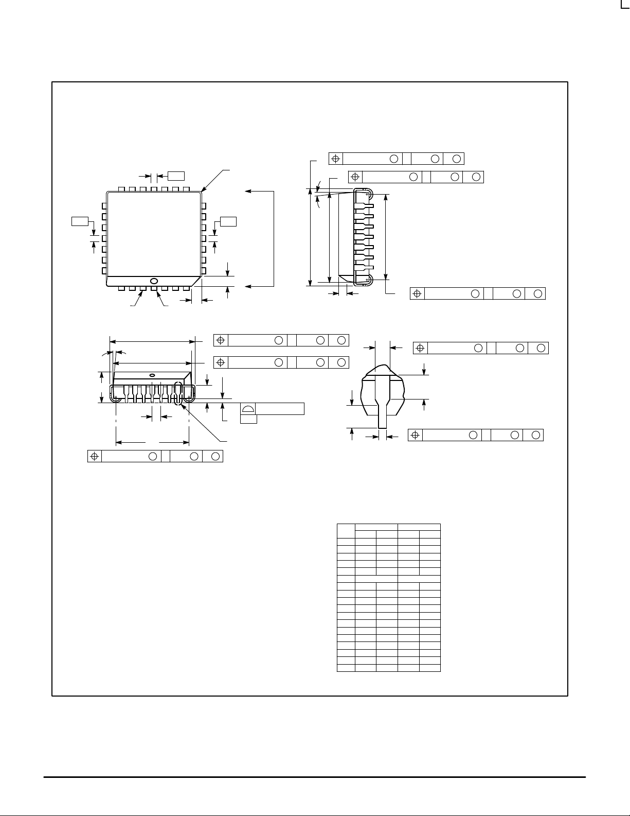
OUTLINE DIMENSIONS
FN SUFFIX
PLASTIC PLCC PACKAGE
CASE 776–02
ISSUE D
0.007 (0.180) T L
–M
SNSM
0.007 (0.180) T L
–M
SNSM
0.007 (0.180) T L
–M
SNSM
0.010 (0.250) T L
–M
SNSS
0.007 (0.180) T L
–M
SNSM
0.010 (0.250) T L
–M
SNSS
0.007 (0.180) T L
–M
SNSM
0.007 (0.180) T L
–M
SNSM
0.004 (0.100)
SEATING
PLANE
-T-
12.32
12.32
4.20
2.29
0.33
0.66
0.51
0.64
11.43
11.43
1.07
1.07
1.07
—
2
°
10.42
1.02
12.57
12.57
4.57
2.79
0.48
0.81
—
—
11.58
11.58
1.21
1.21
1.42
0.50
10
°
10.92
—
1.27 BSC
A
B
C
E
F
G
H
J
K
R
U
V
W
X
Y
Z
G1
K1
MIN MINMAX MAX
INCHES MILLIMETERS
DIM
NOTES:
1. DATUMS -L-, -M-, AND -N- DETERMINED
WHERE TOP OF LEAD SHOULDER EXITS
PLASTIC BODY AT MOLD PARTING LINE.
2. DIM G1, TRUE POSITION TO BE MEASURED
AT DATUM -T-, SEATING PLANE.
3. DIM R AND U DO NOT INCLUDE MOLD FLASH.
ALLOWABLE MOLD FLASH IS 0.010 (0.250)
PER SIDE.
4. DIMENSIONING AND TOLERANCING PER ANSI
Y14.5M, 1982.
5. CONTROLLING DIMENSION: INCH.
6. THE PACKAGE TOP MAY BE SMALLER THAN
THE PACKAGE BOTTOM BY UP TO 0.012
(0.300). DIMENSIONS R AND U ARE
DETERMINED AT THE OUTERMOST
EXTREMES OF THE PLASTIC BODY
EXCLUSIVE OF MOLD FLASH, TIE BAR
BURRS, GATE BURRS AND INTERLEAD
FLASH, BUT INCLUDING ANY MISMATCH
BETWEEN THE TOP AND BOTTOM OF THE
PLASTIC BODY.
7. DIMENSION H DOES NOT INCLUDE DAMBAR
PROTRUSION OR INTRUSION. THE DAMBAR
PROTRUSION(S) SHALL NOT CAUSE THE H
DIMENSION TO BE GREATER THAN 0.037
(0.940). THE DAMBAR INTRUSION(S) SHALL
NOT CAUSE THE H DIMENSION TO BE
SMALLER THAN 0.025 (0.635).
VIEW S
B
U
Z
G1
X
VIEW D-D
H
K
F
VIEW S
G
C
Z
A
R
E
J
0.485
0.485
0.165
0.090
0.013
0.026
0.020
0.025
0.450
0.450
0.042
0.042
0.042
—
2
°
0.410
0.040
0.495
0.495
0.180
0.110
0.019
0.032
—
—
0.456
0.456
0.048
0.048
0.056
0.020
10
°
0.430
—
0.050 BSC
-N-
Y BRK
D
D
W
-M-
-L-
28 1
V
G1
K1

MC10E016 MC100E016
MOTOROLA ECLinPS and ECLinPS Lite
DL140 — Rev 4
2–8
Motorola reserves the right to make changes without further notice to any products herein. Motorola makes no warranty , representation or guarantee regarding
the suitability of its products for any particular purpose, nor does Motorola assume any liability arising out of the application or use of any product or circuit, and
specifically disclaims any and all liability , including without limitation consequential or incidental damages. “Typical” parameters which may be provided in Motorola
data sheets and/or specifications can and do vary in different applications and actual performance may vary over time. All operating parameters, including “Typicals”
must be validated for each customer application by customer’s technical experts. Motorola does not convey any license under its patent rights nor the rights of
others. Motorola products are not designed, intended, or authorized for use as components in systems intended for surgical implant into the body, or other
applications intended to support or sustain life, or for any other application in which the failure of the Motorola product could create a situation where personal injury
or death may occur. Should Buyer purchase or use Motorola products for any such unintended or unauthorized application, Buyer shall indemnify and hold Motorola
and its officers, employees, subsidiaries, affiliates, and distributors harmless against all claims, costs, damages, and expenses, and reasonable attorney fees
arising out of, directly or indirectly, any claim of personal injury or death associated with such unintended or unauthorized use, even if such claim alleges that
Motorola was negligent regarding the design or manufacture of the part. Motorola and are registered trademarks of Motorola, Inc. Motorola, Inc. is an Equal
Opportunity/Affirmative Action Employer.
How to reach us:
USA/EUROPE/Locations Not Listed: Motorola Literature Distribution; JAPAN: Nippon Motorola Ltd.; Tatsumi–SPD–JLDC, 6F Seibu–Butsuryu–Center,
P.O. Box 20912; Phoenix, Arizona 85036. 1–800–441–2447 or 602–303–5454 3–14–2 Tatsumi Koto–Ku, Tokyo 135, Japan. 03–81–3521–8315
MFAX: RMFAX0@email.sps.mot.com – TOUCHTONE 602–244–6609 ASIA/PACIFIC: Motorola Semiconductors H.K. Ltd.; 8B Tai Ping Industrial Park,
INTERNET: http://Design–NET.com 51 Ting Kok Road, Tai Po, N.T., Hong Kong. 852–26629298
MC10E016/D
*MC10E016/D*
◊
 Loading...