

Motorola MBRV7030CTL Datasheet
SEMICONDUCTOR TECHNICAL DATA
Order this document
by MBRV7030CTL/D
Motorola Preferred Device
D3PAK Power Surface Mount Package
Employing the Schottky Barrier principle in a large area metal–to–silicon power
rectifier. Features epitaxial construction with oxide passivation and metal overlay
contact. Ideally suited for low voltage, high frequency switching power supplies;
free wheeling diodes and polarity protection diodes.
• Compact Package Ideal for Automated Handling
• Short Heat Sink Tab Manufactured — Not Sheared
• Highly Stable Oxide Passivated Junction
• Guardring for Over–voltage Protection
• Low Forward Voltage Drop
• Monolithic Dual Die Construction. May be Paralleled for High Current Output.
Mechanical Characteristics:
• Case: Epoxy, Molded
• Weight: 2 Grams (approximately)
• Finish: All External Surfaces Corrosion Resistant and Terminal Leads are
Readily Solderable
• Maximum Temperature of 260°C for 10 Seconds for Soldering
• Shipped 29 Units per Plastic Tube
• Marking: MBRV7030CTL
MAXIMUM RATINGS
Rating Symbol Value Unit
Peak Repetitive Reverse Voltage
Working Peak Reverse Voltage
DC Blocking Voltage
Average Rectified Forward Current Per Leg
(At Rated VR, TC = 135°C) Per Package
Peak Repetitive Forward Current Per Leg
(At Rated VR, Square Wave, 20 kHz, TC = 135°C)
Non–Repetitive Peak Surge Current Per Package
(Surge applied at rated load conditions, halfwave, single phase, 60 Hz)
Storage / Operating Case Temperature T
Operating Junction Temperature T
Voltage Rate of Change (Rated VR, TJ = 25°C) dv/dt 10,000
THERMAL CHARACTERISTICS
Thermal Resistance — Junction–to–Case Per Leg
Thermal Resistance — Junction–to–Ambient (2) Per Leg
ELECTRICAL CHARACTERISTICS
Maximum Instantaneous Forward Voltage (1), see Figure 2 Per Leg
(IF = 35 A, TJ = 25°C)
(IF = 70 A, TJ = 25°C)
(IF = 35 A, TJ = 100°C)
Maximum Instantaneous Reverse Current, see Figure 4 Per Leg
(Rated VR, TJ = 25°C)
(Rated VR, TJ = 100°C)
(1) Pulse Test: Pulse Width ≤ 250 µs, Duty Cycle ≤ 2%
(2) Rating applies when using minimum pad size, FR4 PC Board
Designer’s Data for “Worst Case” Conditions — The Designer’s Data Sheet permits the design of most circuits entirely from the information presented. SOA Limit
curves — representing boundaries on device characteristics — are given to facilitate “worst case” design.
Designer’s and Switchmode are trademarks of Motorola, Inc.
Preferred devices are Motorola recommended choices for future use and best overall value.
1
3
2
SCHOTTKY BARRIER
RECTIFIER
70 AMPERES
30 VOLTS
1
3
CASE 433A–01, Style 1
V
RRM
V
RWM
V
R
I
O
I
FRM
I
FSM
, TC– 55 to 150 °C
stg
J
R
q
JC
R
q
JA
V
F
I
R
D3PAK
30 V
35
70
70 A
500 A
– 55 to 150 °C
0.59
54
0.50
0.62
0.47
2.0
40
2
A
V/ms
°C/W
V
mA
Motorola TMOS Power MOSFET Transistor Device Data
Motorola, Inc. 1997
1
MBRV7030CTL
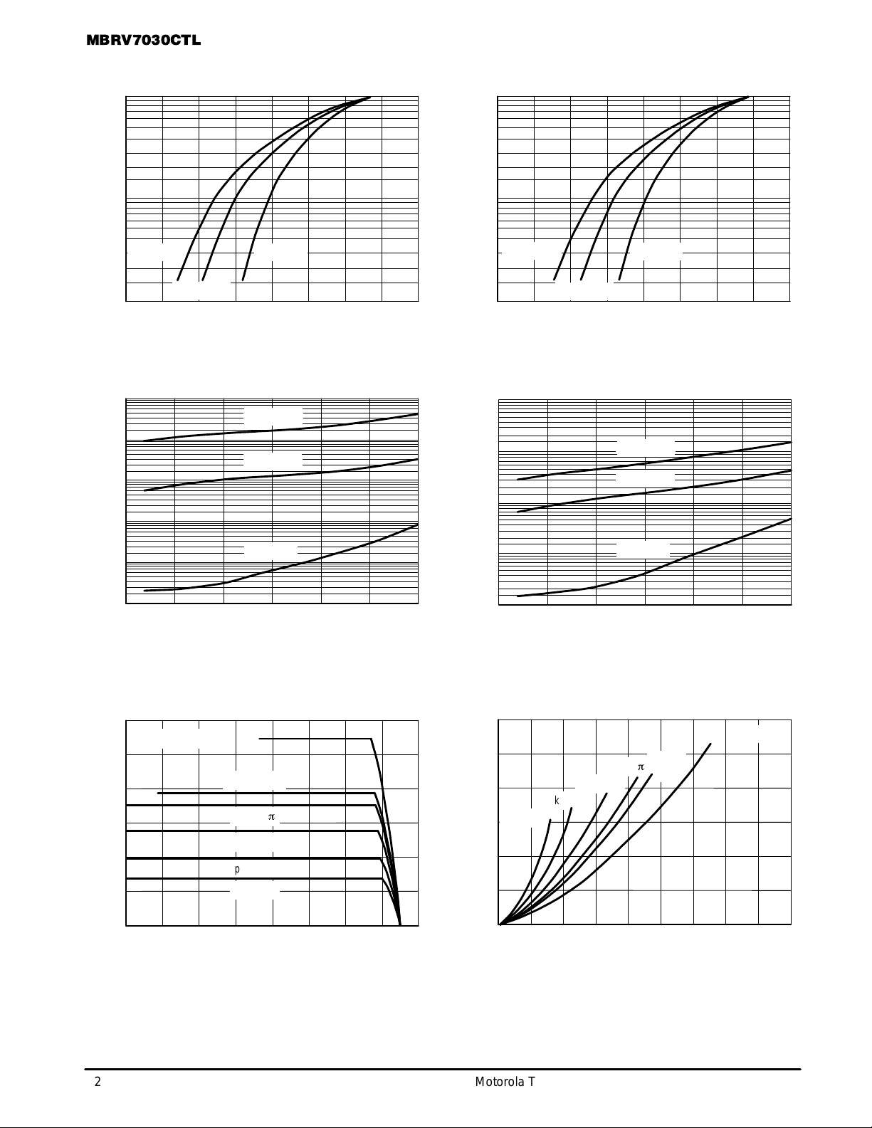
TYPICAL ELECTRICAL CHARACTERISTICS
100
10
1.0
, INSTANTANEOUS FORWARD CURRENT (AMPS)
F
I
1.0
0.1
0.01
0.001
, REVERSE CURRENT (AMPS)
R
I
0.0001
0.00001
TJ = 25
TJ = 150
°C
TJ = 100
°C
VF, INSTANTANEOUS FORWARD VOLTAGE (VOLTS)
°C
Figure 1. T ypical Forward Voltage
TJ = 150
°C
TJ = 100
°C
TJ = 25
°C
VR, REVERSE VOLTAGE (VOLTS)
100
10
TJ = 150
°C
1.0
0.80.60.40.20
, INSTANTANEOUS FORWARD CURRENT (AMPS)
F
I
VF, MAXIMUM INSTANTANEOUS FORWARD VOLTAGE (VOLTS)
TJ = 100
°C
TJ = 25
°C
0.80.60.40.20
Figure 2. Maximum Forward V oltage
10
TJ = 150
TJ = 100
TJ = 25
°C
°C
°C
3020100
1.0
0.1
0.01
, MAXIMUM REVERSE CURRENT (AMPS)
R
I
3020100
0.001
VR, REVERSE VOLTAGE (VOLTS)
60
50
40
30
20
10
, AVERAGE FORW ARD CURRENT (AMPS)
O
I
0
Figure 3. T ypical Reverse Current
FREQ = 20 kHz
dc
square wave
Ipk/Io =
p
Ipk/Io = 5
Ipk/Io = 10
Ipk/Io = 20
TC, CASE TEMPERATURE (°C)
Figure 5. Current Derating (Per Leg)
Figure 4. Maximum Reverse Current
30
25
20
Ipk/Io = 20
15
10
5
, AVERAGE POWER DISSIPA TION (WATTS)
FO
P
160140120100806040200
0
Ipk/Io = 10
IO, AVERAGE FORW ARD CURRENT (AMPS)
Ipk/Io =
Ipk/Io = 5
p
square
wave
dc
TJ = 150
°C
7550250
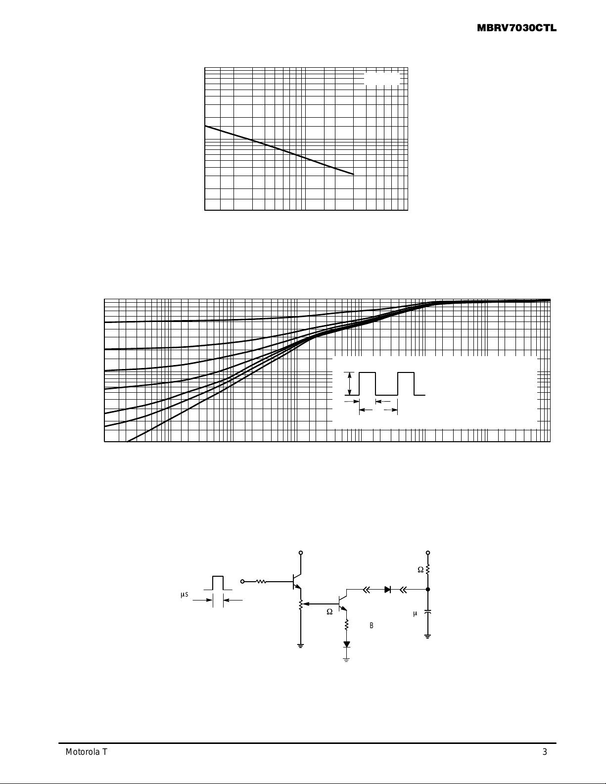
Figure 6. Forward Power Dissipation (Per Leg)
2
Motorola TMOS Power MOSFET Transistor Device Data
1.0
TYPICAL ELECTRICAL CHARACTERISTICS
100,000
10,000
C, CAPACITANCE (pF)
1,000
1.0 10 100
VR, REVERSE VOLTAGE (VOLTS)
Figure 7. Capacitance
SAFE OPERATING AREA
MBRV7030CTL
TJ = 25°C
P
0.1
r(t), NORMALIZED EFFECTIVE
TRANSIENT THERMAL RESISTANCE
0.01
0.000001 0.00001 0.0001 0.001 0.01 0.1 1.0 10
t, TIME (SECONDS)
(pk)
t
1
t
2
DUTY CYCLE, D = t1/t
R
(t) = r(t) R
θ
JC
D CURVES APPLY FOR POWER
PULSE TRAIN SHOWN
READ TIME AT t
T
J(pk)
2
– TC = P
θ
(pk)
JC
1
Figure 8. Thermal Response
+ 150 V,
10 mAdc
2 k
W
4
m
F
+
2 ms
1 kHz
12 V
100
CURRENT
AMPLITUDE
ADJUST
0–10 AMPS
V
CC
12 Vdc
2N2222
100
W
CARBON
D.U.T.
2N6277
1 CARBON
1N5817
R
(t)
θ
JC
Figure 9. T est Circuit for Repetitive
Reverse Current
Motorola TMOS Power MOSFET Transistor Device Data
3
 Loading...