

Motorola MBRS1100T3 Datasheet
SEMICONDUCTOR TECHNICAL DATA
Surface Mount Power Package
Schottky Power Rectifiers employ the use of the Schottky Barrier principle in
a large area metal-to-silicon power diode. State-of-the-art geometry features
epitaxial construction with oxide passivation and metal overlay contact. Ideally
suited for low voltage, high frequency rectification, or as free wheeling and
polarity protection diodes, in surface mount applications where compact size
and weight are critical to the system. These state-of-the-art devices have the
following features:
• Small Compact Surface Mountable Package with J-Bend Leads
• Rectangular Package for Automated Handling
• Highly Stable Oxide Passivated Junction
• High Blocking Voltage — 100 Volts
• 150°C Operating Junction Temperature
• Guardring for Stress Protection
Mechanical Characteristics
• Case: Epoxy, Molded
• Weight: 95 mg (approximately)
• Finish: All External Surfaces Corrosion Resistant and Terminal Leads are
Readily Solderable
• Lead and Mounting Surface Temperature for Soldering Purposes: 260°C
Max. for 10 Seconds
• Shipped in 12 mm Tape and Reel, 2500 units per reel
• Polarity: Notch in Plastic Body Indicates Cathode Lead
• Marking: B1 10
Order this document
by MBRS1100T3/D
Motorola Preferred Device
SCHOTTKY BARRIER
RECTIFIER
1.0 AMPERE
100 VOL TS
CASE 403A–03
MAXIMUM RATINGS
Rating Symbol Value Unit
Peak Repetitive Reverse Voltage
Working Peak Reverse Voltage
DC Blocking Voltage
Average Rectified Forward Current TL = 120°C
TL = 100°C
Nonrepetitive Peak Surge Current
(Surge applied at rated load conditions halfwave, single phase, 60 Hz)
Operating Junction Temperature T
Voltage Rate of Change dv/dt 10 V/ns
V
RRM
V
RWM
V
I
F(AV)
I
FSM
100 Volts
R
1.0
2.0
50 Amps
J
– 65 to +150 °C
Amps
THERMAL CHARACTERISTICS
Thermal Resistance — Junction to Lead (TL = 25°C) R
θJL
22 °C/W
ELECTRICAL CHARACTERISTICS
Maximum Instantaneous Forward Voltage (1)
(iF = 1.0 A, TJ = 25°C)
Maximum Instantaneous Reverse Current (1)
(Rated dc Voltage, TJ = 25°C)
(Rated dc Voltage, TJ = 100°C)
(1) Pulse Test: Pulse Width = 300 µs, Duty Cycle ≤2.0%.
Preferred devices are Motorola recommended choices for future use and best overall value.
Designer’s Data for “Worst Case” Conditions — The Designer’s Data Sheet permits the design of most circuits entirely from the information presented. SOA Limit
curves — representing boundaries on device characteristics — are given to facilitate “worst case” design.
V
F
i
R
0.75 Volts
mA
0.5
5.0
Rev 2
Rectifier Device Data
Motorola, Inc. 1996
1
MBRS1100T3
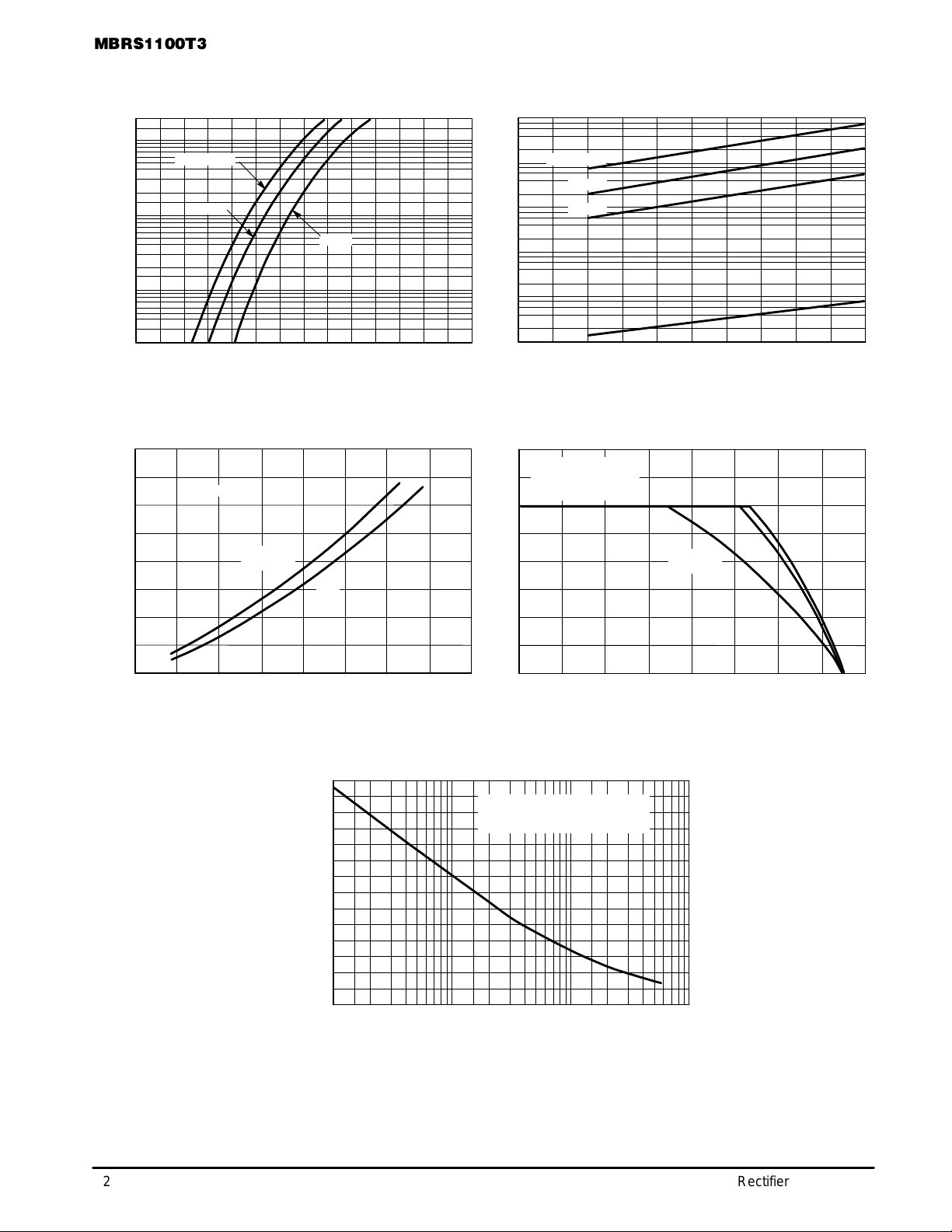
TYPICAL ELECTRICAL CHARACTERISTICS
20
10
5
2
1
0.5
0.2
0.1
0.05
F
0.02
i , INSTANTANEOUS FORWARD CURRENT (AMPS)
TJ = 150°C
100°C
25°C
0 0.1 0.2 0.3 0.4 0.5 0.6 0.7 0.8 0.9 1 1.1 1.2 1.3 1.4
vF, INSTANTANEOUS VOLTAGE (VOLTS)
Figure 1. Typical Forward Voltage Figure 2. Typical Reverse Current
3.2
2.8
2.4
2.0
1.6
1.2
TJ = 100°C
SQUARE
WAVE
DC
1 K
400
µ
, REVERSE CURRENT ( A)
R
I
0.04
0.02
0.01
200
100
40
20
10
0.4
0.2
0.1
4.0
3.5
3.0
2.5
2.0
1.5
T
= 150°C
J
125°C
100°C
4
2
1
0 102030405060708090100
VR, REVERSE VOLTAGE (VOLTS)
RATED VR APPLIED
R
= 22°C/W
θ
JL
TJ = 100
°
C
DC
SQUARE
WAVE
0.8
0.4
F(AV)
P , AVERAGE POWER DISSIPATION (WATTS)
0
0 0.5 1.0 1.5 2.0 2.5 3.0 3.5 4.0
I
, AVERAGE FORW ARD CURRENT (AMPS)
F(AV)
Figure 3. Power Dissipation Figure 4. Current Derating, Lead
280
260
240
220
200
180
160
140
120
100
80
C, CAPACITANCE (pF)
60
40
20
0
0.1 0.2 0.5 1 2 5 10 20 50 100
Figure 5. T ypical Capacitance
1.0
0.5
F(AV)
I , AVERAGE FORWARD CURRENT (AMPS)
0
0 20 40 60 80 100 120 140 160
NOTE: TYPICAL CAPACITANCE
NOTE: AT 0 V = 270 pF
VR, REVERSE VOLTAGE (VOLTS)
TL, LEAD TEMPERATURE (°C)
2
Rectifier Device Data
 Loading...