

Motorola MBRF1045 Datasheet
SEMICONDUCTOR TECHNICAL DATA
Order this document
by MBRF1045/D
The SWITCHMODE Power Rectifier employs the Schottky Barrier principle in
a large area metal–to–silicon power diode. State–of–the–art geometry features
epitaxial construction with oxide passivation and metal overlay contact. Ideally
suited for use as rectifiers in very low–voltage, high–frequency switching power
supplies, free wheeling diodes and polarity protection diodes.
• Highly Stable Oxide Passivated Junction
• Very Low Forward Voltage Drop
• High Junction Temperature Capability
• High dv/dt Capability
• Excellent Ability to Withstand Reverse Avalanche Energy
Transients
• Guardring for Stress Protection
• Epoxy Meets UL94, VO at 1/8″
• Electrically Isolated. No Isolation Hardware Required.
• UL Recognized File #E69369
Mechanical Characteristics
• Case: Epoxy, Molded
• Weight: 1.9 grams (approximately)
• Finish: All External Surfaces Corrosion Resistant and Terminal
Leads are Readily Solderable
• Lead Temperature for Soldering Purposes: 260°C Max. for 10
Seconds
• Shipped 50 units per plastic tube
• Marking: B1045
(1)
Motorola Preferred Device
SCHOTTKY BARRIER
RECTIFIER
10 AMPERES
45 VOLTS
12
1
2
CASE 221E–01
ISOLATED TO–220
MAXIMUM RATINGS
Rating Symbol Value Unit
Peak Repetitive Reverse Voltage
Working Peak Reverse Voltage
DC Blocking Voltage
Average Rectified Forward Current (Rated VR), TC = 135°C I
Peak Repetitive Forward Current
(Rated VR, Square Wave, 20 kHz), TC = 135°C
Non–repetitive Peak Surge Current
(Surge applied at rated load conditions halfwave, single phase, 60 Hz)
Peak Repetitive Reverse Surge Current (2.0 µs, 1.0 kHz) Figure 6 I
Operating Junction and Storage Temperature TJ, T
Voltage Rate of Change (Rated VR) dv/dt 10000 V/µs
RMS Isolation Voltage (t = 1 second, R.H. ≤ 30%, TA = 25°C)
(2)
Per Figure 8
Per Figure 9
Per Figure 10
(1)
V
RRM
V
RWM
V
F(AV)
I
FRM
I
FSM
RRM
V
iso1
V
iso2
V
iso3
45 Volts
R
10 Amps
20 Amps
150 Amps
1.0 Amp
stg
– 65 to +150 °C
4500
3500
1500
THERMAL CHARACTERISTICS
Maximum Thermal Resistance, Junction to Case R
Lead Temperature for Soldering Purposes: 1/8″ from Case for 5 seconds T
(1) UL Recognized mounting method is per Figure 9.
(2) Proper strike and creepage distance must be provided.
SWITCHMODE is a trademark of Motorola, Inc.
Preferred devices are Motorola recommended choices for future use and best overall value.
θJC
L
4.0 °C/W
260 °C
Volts
Rev 1
Rectifier Device Data
Motorola, Inc. 1996
1
MBRF1045
ELECTRICAL CHARACTERISTICS
Characteristic Symbol Max Unit
Maximum Instantaneous Forward Voltage (3)
(iF = 20 Amp, TC = 25°C)
(iF = 20 Amp, TC = 125°C)
(iF = 10 Amp, TC = 125°C)
Maximum Instantaneous Reverse Current (3)
(Rated DC Voltage, TC = 25°C)
(Rated DC Voltage, TC = 125°C)
(3) Pulse Test: Pulse Width = 300 µs, Duty Cycle ≤ 2.0%
v
F
i
R
0.84
0.72
0.57
0.1
15
Volts
mA
100
70
50
30
20
10
7
5
3
2
1
0.7
0.5
0.3
0.2
0.1
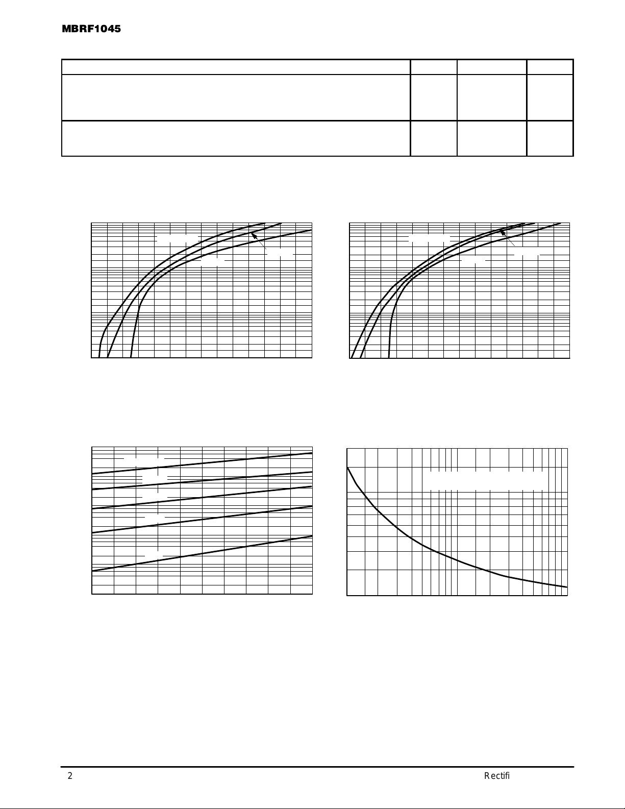
, INSTANTANEOUS FORWARD CURRENT (AMPS)
F
i
100
10
1
0.1
TJ = 150°C
100°C
25°C
0.2 0.4 0.6 0.8 1 1.2 1.4
vF, INSTANTANEOUS VOLTAGE (VOLTS)
Figure 1. Maximum Forward V oltage
TJ = 150°C
125°C
100°C
75°C
100
70
50
30
20
10
7
5
3
2
1
0.7
0.5
0.3
0.2
0.1
0.2 0.4 0.6 0.8 1 1.2 1.4
, INSTANTANEOUS FORWARD CURRENT (AMPS)
F
i
TJ = 150°C
25°C
vF, INSTANTANEOUS VOLTAGE (VOLTS)
Figure 2. T ypical Forward Voltage
200
100
70
50
TJ = 125°C, V
BETWEEN EACH CYCLE OF SURGE
MAY BE APPLIED
RRM
100°C
, REVERSE CURRENT (mA)
R
I
0.001
2
0.01
25°C
30
, PEAK HALF-WAVE CURRENT (AMPS)
FSM
I
10020304050
VR, REVERSE VOLTAGE (VOLTS)
20
Figure 3. Maximum Reverse Current
21 5 10 20 100
3 7 30 50 70
NUMBER OF CYCLES AT 60 Hz
Figure 4. Maximum Surge Capability
Rectifier Device Data
 Loading...