

Motorola MBRB4030 Datasheet
SEMICONDUCTOR TECHNICAL DATA
Order this document
by MBRB4030/D
Using the Schottky Barrier principle with a proprietary barrier metal. These
state–of–the–art devices have the following features:
• Guardring for Stress Protection
• Maximum Die Size
• 150°C Operating Junction Temperature
• Short Heat Sink Tab Manufactured – Not Sheared
Mechanical Characteristics
• Case: Epoxy, Molded
• Weight: 1.7 Grams (approximately)
• Finish: All External Surfaces Corrosion Resistant and Terminal
Leads Readily Solderable
• Shipped 50 Units per Plastic Tube
• Available in 24 mm Tape and Reel, 800 Units per 13
Adding a “T4” Suffix to the Part Number
• Marking: B4030
″ Reel by
1
3
4
MAXIMUM RATINGS
Rating Symbol Value Unit
Peak Repetitive Reverse Voltage
Working Peak Reverse Voltage
DC Blocking Voltage
Average Rectified Forward Current
(At Rated VR) TC = +115°C (1)
Peak Repetitive Forward Current
(At Rated VR, Square Wave, 20 kHz) TC = + 112°C
Nonrepetitive Peak Surge Current
(Surge Applied at Rated Load Conditions Halfwave, Single Phase, 60 Hz)
Peak Repetitive Reverse Surge Current (2.0 µs, 1.0 kHz) I
Storage Temperature T
Operating Junction Temperature T
Voltage Rate of Change (Rated VR) dv/dt 10,000 V/µs
Reverse Energy (Unclamped Inductive Surge) (Inductance = 3 mH), Tc = 25°C W 600 mJ
THERMAL CHARACTERISTICS
Thermal Resistance – Junction to Case R
Thermal Resistance – Junction to Ambient (2) R
ELECTRICAL CHARACTERISTICS
Maximum Instantaneous Forward V oltage (1 and 3), per Device
(IF = 20 A, TC = + 25°C)
(IF = 20 A, TC = +150°C)
(IF = 40 A, TC = + 25°C)
(IF = 40 A, TC = +150°C)
Maximum Instantaneous Reverse Current (3), per Device
(Rated DC Voltage, TC = + 25°C)
(Rated DC Voltage, TC = +125°C)
(1) Rating applies when pins 1 and 3 are connected.
(2) Rating applies when surface mounted on the miniumum pad size recommended.
(3) Pulse Test: Pulse Width = 300 µs, Duty Cycle ≤ 2.0%
SWITCHMODE is a trademark of Motorola, Inc.
Preferred devices are Motorola recommended choices for future use and best overall value.
V
RRM
V
RWM
V
I
F(AV)
I
FRM
I
FSM
RRM
θJC
θJA
V
I
R
stg
J
F
R
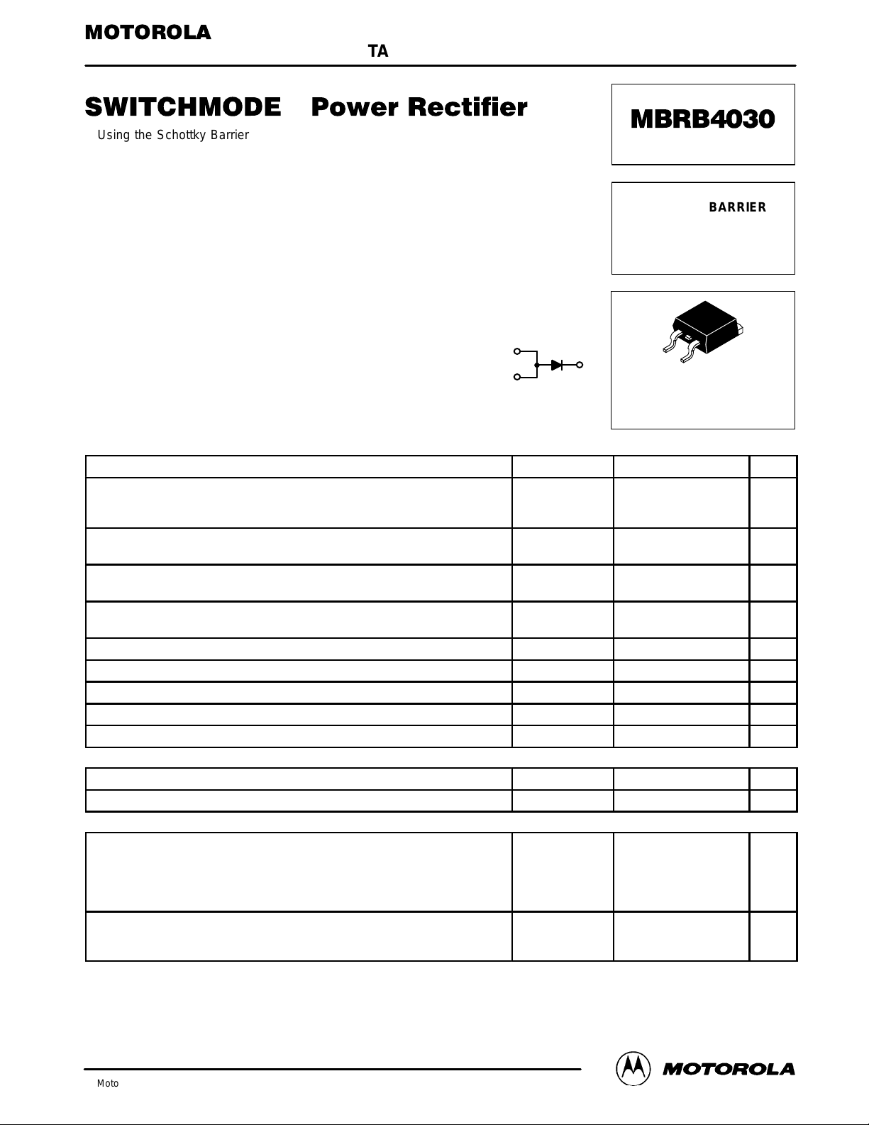
Motorola Preferred Device
SCHOTTKY BARRIER
RECTIFIER
40 AMPERES
30 VOLTS
4
1
3
CASE 418B–02
D2PAK
30
40 A
80 A
300 A
2.0 A
– 65 to +150 °C
– 65 to +150 °C
1.0 °C/W
50 °C/W
0.46
0.34
0.55
0.45
0.35
150
V
V
mA
Rectifier Device Data
Motorola, Inc. 1996
1

MBRB4030
7
ELECTRICAL CHARACTERISTICS
100
(PIN 1 SHORTED TO PIN 3)
, INSTANTANEOUS FORWARD CURRENT (mA)
F
I
0.01
10
1.0
0.1
1.0
0.1
TJ = 150°C
100°C
VF, INSTANTANEOUS VOLTAGE (V)
25°C
Figure 1. Maximum Forward V oltage
TJ = 150°C
100°C
100
10
1.0
(PIN 1 SHORTED TO PIN 3)
, INSTANTANEOUS FORWARD CURRENT (mA)
F
I
0.80.60.40.20
0.70.50.30.1 0.50.30.2
0.1
VF, INSTANTANEOUS VOLTAGE (V)
Figure 2. T ypical Forward Voltage
1.0
0.1
0.01
100°C
TJ = 150°C
25°C
TJ = 150°C
100°C
0.60.40.10
0.
, REVERSE CURRENT (A)
R
I
10
10
10
–3
–4
–5
25°C
205 20155
VR, REVERSE VOLTAGE (V)
Figure 3. Maximum Reverse Current
4
10
C, CAPACITANCE (pF)
1000
1
–3
10
, REVERSE CURRENT (A)
R
I
–4
10
–5
10
302515100
TYPICAL
VR, REVERSE VOLTAGE (V)
MAXIMUM
25°C
3025100
VR, REVERSE VOLTAGE (V)
Figure 4. T ypical Reverse Current
TJ = 25°C
10
Figure 5. Maximum and T ypical Capacitance
2
Rectifier Device Data
 Loading...