SEMICONDUCTOR TECHNICAL DATA
Order this document
by MBR150/D
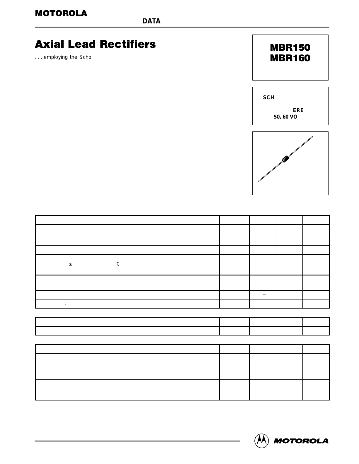
. . . employing the Schottky Barrier principle in a large area metal–to–silicon
power diode. State–of–the–art geometry features epitaxial construction with
oxide passivation and metal overlap contact. Ideally suited for use as rectifiers
in low–voltage, high–frequency inverters, free wheeling diodes, and polarity
protection diodes.
• Low Reverse Current
• Low Stored Charge, Majority Carrier Conduction
• Low Power Loss/High Efficiency
• Highly Stable Oxide Passivated Junction
Mechanical Characteristics:
• Case: Epoxy, Molded
• Weight: 0.4 gram (approximately)
• Finish: All External Surfaces Corrosion Resistant and Terminal Leads are
Readily Solderable
• Lead and Mounting Surface Temperature for Soldering Purposes: 220°C
Max. for 10 Seconds, 1/16″ from case
• Shipped in plastic bags, 1000 per bag
• Available Tape and Reeled, 5000 per reel, by adding a “RL’’ suf fix to the
part number
• Polarity: Cathode Indicated by Polarity Band
• Marking: B150, B160
MAXIMUM RATINGS
Rating Symbol MBR150 MBR160 Unit
Peak Repetitive Reverse Voltage
Working Peak Reverse Voltage
DC Blocking Voltage
RMS Reverse Voltage V
Average Rectified Forward Current (2)
(V
R(equiv)
see Note 3, TA = 55°C)
Nonrepetitive Peak Surge Current
(Surge applied at rated load conditions, halfwave, single phase, 60 Hz, TL = 70°C)
Operating and Storage Junction Temperature Range (Reverse Voltage applied) TJ, T
Peak Operating Junction Temperature (Forward Current applied) T
THERMAL CHARACTERISTICS (Notes 3 and 4)
Thermal Resistance, Junction to Ambient R
ELECTRICAL CHARACTERISTICS (T
Maximum Instantaneous Forward Voltage (1)
(iF = 0.1 A)
(iF = 1 A)
(iF = 3 A)
Maximum Instantaneous Reverse Current @ Rated dc Voltage (1)
(TL = 25°C)
(TL = 100°C)
(1) Pulse Test: Pulse Width = 300 µs, Duty Cycle ≤ 2.0%.
(2) Lead Temperature reference is cathode lead 1/32″ from case.
v 0.2 VR(dc), TL = 90°C, R
Characteristic Symbol Max Unit
Characteristic Symbol Max Unit
= 80°C/W, P.C. Board Mounting,
θJA
= 25°C unless otherwise noted) (2)
L
V
RRM
V
RWM
V
R
R(RMS)
I
O
I
FSM
stg
J(pk)
θJA
v
F
i
R
MBR160 is a
Motorola Preferred Device
SCHOTTKY BARRIER
RECTIFIERS
1 AMPERE
50, 60 VOL TS
CASE 59–04
PLASTIC
50 60 Volts
35 42 Volts
1 Amp
25 (for one cycle) Amps
*
65 to +150 °C
150 °C
80 °C/W
0.550
0.750
1.000
0.5
5
Volt
mA
Preferred devices are Motorola recommended choices for future use and best overall value.
Rev 1
Rectifier Device Data
Motorola, Inc. 1996
1

10
7.0
5.0
3.0
2.0
1.0
0.7
0.5
0.3
0.2
TJ = 150°C
100°C
25°C
10
5.0
2.0
1.0
0.5
0.2
TJ = 150°C
125°C
100°C
75°C
0.1
0.05
0.02
0.01
, REVERSE CURRENT (mA)
R
I
0.005
25°C
0.002
0.001
50 6010 20 30
40 700
VR, REVERSE VOLTAGE (VOLTS)
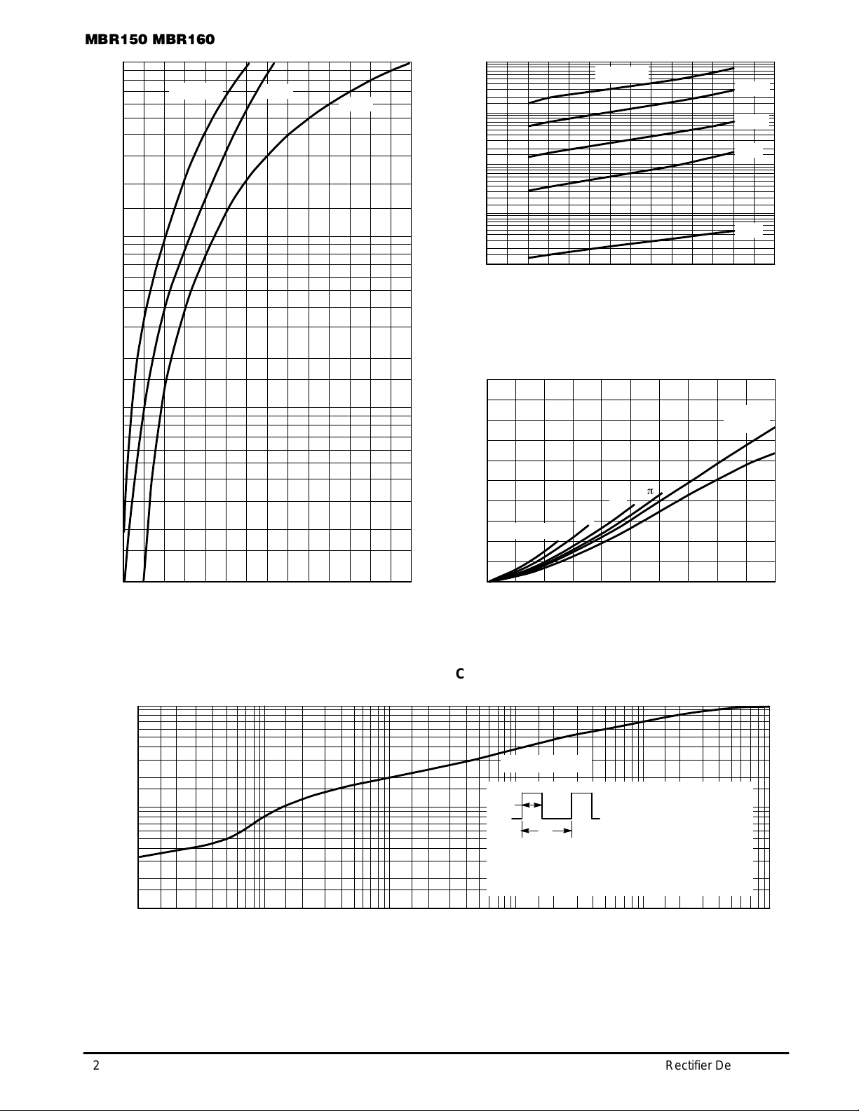
Figure 2. T ypical Reverse Current*
*The curves shown are typical for the highest voltage device in the voltage grouping. Typical reverse current for lower voltage selections can
be estimated from these same curves if VR is sufficiently below rated VR.
5.0
0.1
, INSTANTANEOUS FORWARD CURRENT (AMPS)
F
i
4.0
0.07
, AVERAGE FORW ARD
F(AV)
P
3.0
2.0
1.0
POWER DISSIPATION (WATTS)
0
p
5
10
IPK/IAV = 20
1.00
I
, AVERAGE FORW ARD CURRENT (AMPS)
F(AV )
2.0
3.0 4.0 5.0
Figure 3. Forward Power Dissipation
0.05
0.03
0.02
0
0.60.2 0.4 0.8 1.0
1.2
1.4
1.6
vF, INSTANTANEOUS VOLTAGE (VOLTS)
Figure 1. T ypical Forward Voltage
THERMAL CHARACTERISTICS
1.0
0.7
0.5
0.3
0.2
0.1
0.07
(NORMALIZED)
0.05
0.03
0.02
r(t), TRANSIENT THERMAL RESIST ANCE
0.01
0.1 0.2 0.5 1.0 2.0 5.0 10 20 50 100 200 500 1 k 2 k 5 k 10 k
t, TIME (ms)
Figure 4. Thermal Response
Z
= Z
θ
JL
P
pk
t
1
[D + (1 – D)
θ
JL
• r(t)
•
P
pk
DUTY CYCLE, D = tp/t
PEAK POWER, Ppk, is peak of an
equivalent square power pulse.
TIME
r(t1 + tp) + r(tp) – r(t1)]
θ
JL(t)
t
p
∆
TJL = Ppk • R
where
∆
TJL = the increase in junction temperature above the lead temperature
r(t) = normalized value of transient thermal resistance at time, t, from Figure 4, i.e.:
r(t) = r(t1 + tp) = normalized value of transient thermal resistance at time, t
1
+ tp.
1
SQUARE
WAVE
dc
2
Rectifier Device Data
 Loading...