

Page 1
MOTOROLA
查询MAC12/D供应商
SEMICONDUCTOR TECHNICAL DATA
Order this document
by MAC12/D
MAC12
SERIES
*Motorola preferred devices
*
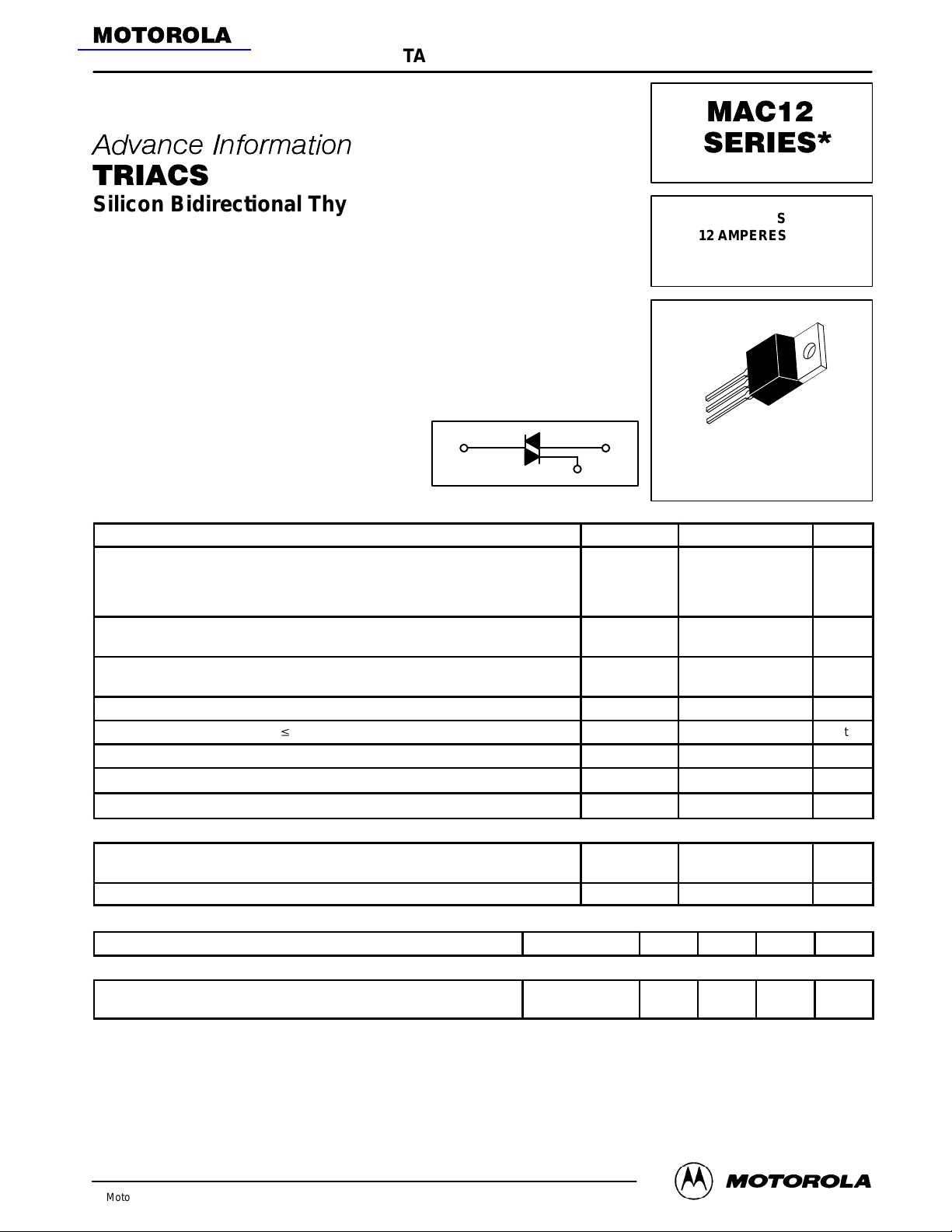
TRIACS
Silicon Bidirectional Thyristors
Designed for high performance full–wave ac control applications where high
noise immunity and commutating di/dt are required.
• Blocking Voltage to 800 Volts
• On–State Current Rating of 12 Amperes RMS at 70°C
• Uniform Gate Trigger currents in Three Modes
• High Immunity to dv/dt — 250 V/µs minimum at 125°C
• High Commutating di/dt — 6.5 A/ms minimum at 125°C
• Industry Standard TO–220 AB Package
• High Surge Current Capability — 120 Amperes
MT2
MT1
G
MAXIMUM RATINGS (TJ = 25°C unless otherwise noted)
Parameter Symbol Value Unit
Peak Repetitive Off–State V oltage
(TJ = –40 to 125°C, Sine Wave, 50 to 60 Hz, Gate Open) MAC12D
On–State RMS Current
(Full Cycle Sine Wave, 60 Hz, TC = 70°C)
Peak Non–repetitive Surge Current
(One Full Cycle, 60 Hz, TJ = 125°C)
Circuit Fusing Consideration (t = 8.3 ms) I2t 41 A2sec
Peak Gate Power (Pulse Width v1.0 µs, TC = 80°C) P
Average Gate Power (t = 8.3 ms, TC = 80°C) P
Operating Junction Temperature Range T
Storage Temperature Range T
(1)
MAC12M
MAC12N
V
DRM
I
T(RMS)
I
TSM
GM
G(AV)
J
stg
THERMAL CHARACTERISTICS
Thermal Resistance — Junction to Case
Maximum Lead Temperature for Soldering Purposes 1/8″ from Case for 10 Seconds T
ELECTRICAL CHARACTERISTICS (T
— Junction to Ambient
Characteristic
= 25°C unless otherwise noted)
J
Symbol Min Typ Max Unit
R
R
θJC
θJA
L
OFF CHARACTERISTICS
Peak Repetitive Blocking Current TJ = 25°C
(VD = Rated V
(1) V
This document contains information on a new product. Specifications and information herein are subject to change without notice.
Preferred devices are Motorola recommended choices for future use and best overall value.
and V
DRM
not be applied concurrent with negative potential on the anode. Blocking voltages shall not be tested with a constant current source such that the
voltage ratings of the devices are exceeded.
, Gate Open) TJ = 125°C
DRM
for all types can be applied on a continuous basis. Ratings apply for zero or negative gate voltage; positive gate voltage shall
RRM
I
DRM
MT1
MT2
—
—
TRIACS
12 AMPERES RMS
400 thru 800
VOLTS
G
CASE 221A-09
(TO-220AB)
Style 4
400
600
800
12 A
100 A
16 Watts
0.35 Watts
–40 to +125
–40 to +150
2.2
62.5
260 °C
—
—
0.01
2.0
MT2
Volts
°C
°C
°C/W
mA
REV 2
Motorola Thyristor Device Data
Motorola, Inc. 1999
1
Page 2
ELECTRICAL CHARACTERISTICS
Characteristic
ON CHARACTERISTICS
Peak On–State Voltage* (ITM = "17 A) V
Continuous Gate Trigger Current (VD = 12 V, RL = 100 Ω)
MT2(+), G(+)
MT2(+), G(–)
MT2(–), G(–)
Hold Current (VD = 12 V, Gate Open, Initiating Current = "150 mA) I
Latch Current (VD = 24 V, IG = 35 mA)
MT2(+), G(+); MT2(–), G(–)
MT2(+), G(–)
Gate Trigger V oltage (VD = 12 V, RL = 100 Ω)
MT2(+), G(+)
MT2(+), G(–)
MT2(–), G(–)
DYNAMIC CHARACTERISTICS
Rate of Change of Commutating Current*
(VD = 400 V , ITM = 4.4A, Commutating dv/dt = 18 V/ µs, Gate Open,
TJ = 125°C, f = 250 Hz, No Snubber)
Critical Rate of Rise of Off–State V oltage
(VD = Rated V
*Indicates Pulse Test: Pulse Width v2.0 ms, Duty Cycle v2%.
, Exponential Waveform, Gate Open, TJ = 125°C)
DRM
(TJ = 25°C unless otherwise noted)
Symbol Min Typ Max Unit
TM
I
GT
H
I
L
V
GT
(dv/dt)c 6.5 — — A/ms
dv/dt 250 — — V/µs
— — 1.85 Volts
5.0
5.0
5.0
— 20 40 mA
—
—
0.5
0.5
0.5
13
16
18
20
30
0.69
0.77
0.72
35
35
35
50
80
1.5
1.5
1.5
mA
mA
Volts
2 Motorola Thyristor Device Data
Page 3

P ACKAGE DIMENSIONS
SEATING
–T–
PLANE
B
4
Q
123
F
T
A
U
C
S
H
K
Z
L
V
R
J
G
D
N
STYLE 4:
PIN 1. MAIN TERMINAL 1
2. MAIN TERMINAL 2
3. GATE
4. MAIN TERMINAL 2
NOTES:
1. DIMENSIONING AND TOLERANCING PER ANSI
Y14.5M, 1982.
2. CONTROLLING DIMENSION: INCH.
3. DIMENSION Z DEFINES A ZONE WHERE ALL
BODY AND LEAD IRREGULARITIES ARE
ALLOWED.
DIM MIN MAX MIN MAX
A 0.570 0.620 14.48 15.75
B 0.380 0.405 9.66 10.28
C 0.160 0.190 4.07 4.82
D 0.025 0.035 0.64 0.88
F 0.142 0.147 3.61 3.73
G 0.095 0.105 2.42 2.66
H 0.110 0.155 2.80 3.93
J 0.018 0.025 0.46 0.64
K 0.500 0.562 12.70 14.27
L 0.045 0.060 1.15 1.52
N 0.190 0.210 4.83 5.33
Q 0.100 0.120 2.54 3.04
R 0.080 0.110 2.04 2.79
S 0.045 0.055 1.15 1.39
T 0.235 0.255 5.97 6.47
U 0.000 0.050 0.00 1.27
V 0.045 ––– 1.15 –––
Z ––– 0.080 ––– 2.04
MILLIMETERSINCHES
CASE 221A-09
(TO–220AB)
ISSUE Z
Motorola Thyristor Device Data
3
Page 4

Motorola reserves the right to make changes without further notice to any products herein. Motorola makes no warranty , representation or guarantee regarding
the suitability of its products for any particular purpose, nor does Motorola assume any liability arising out of the application or use of any product or circuit, and
specifically disclaims any and all liability, including without limitation consequential or incidental damages. “T ypical” parameters which may be provided in Motorola
data sheets and/or specifications can and do vary in different applications and actual performance may vary over time. All operating parameters, including “Typicals”
must be validated for each customer application by customer’s technical experts. Motorola does not convey any license under its patent rights nor the rights of
others. Motorola products are not designed, intended, or authorized for use as components in systems intended for surgical implant into the body, or other
applications intended to support or sustain life, or for any other application in which the failure of the Motorola product could create a situation where personal injury
or death may occur. Should Buyer purchase or use Motorola products for any such unintended or unauthorized application, Buyer shall indemnify and hold Motorola
and its officers, employees, subsidiaries, affiliates, and distributors harmless against all claims, costs, damages, and expenses, and reasonable attorney fees
arising out of, directly or indirectly, any claim of personal injury or death associated with such unintended or unauthorized use, even if such claim alleges that
Motorola was negligent regarding the design or manufacture of the part. Motorola and are registered trademarks of Motorola, Inc. Motorola, Inc. is an Equal
Opportunity/Affirmative Action Employer.
How to reach us:
USA/EUROPE /Locations Not Listed: Motorola Literature Distribution; JAPAN: Motorola Japan Ltd.; SPD, Strategic Planning Office, 141,
P.O. Box 5405, Denver, Colorado 80217. 1–303–675–2140 or 1–800–441–2447 4–32–1 Nishi–Gotanda, Shinagawa–ku, Tokyo, Japan. 81–3–5487–8488
Customer Focus Center: 1–800–521–6274
Mfax: RMFAX0@email.sps.mot.com – TOUCHTONE 1–602–244–6609 ASIA/PACIFIC: Motorola Semiconductors H.K. Ltd.; Silicon Harbour Centre,
Motorola Fax Back System – US & Canada ONLY 1–800–774–1848 2, Dai King Street, Tai Po Industrial Estate, Tai Po, N.T., Hong Kong.
HOME PAGE: http://motorola.com/sps/
4 Motorola Thyristor Device Data
– http://sps.motorola.com/mfax/ 852–26629298
◊
Mfax is a trademark of Motorola, Inc.
MAC12/D
 Loading...