

Page 1

Professional Radio
GM Series
Controller
Service Information
Issue: September 2000
Page 2

ii
Computer Software Copyrights
The Motorola products described in this manual may include copyrighted Motorola computer programs stored
in semiconductor memories or other media. Laws in the United States and other countries preserve for
Motorola certain exclusive rights for copyrighted computer programs, including the exclusive right to copy or
reproduce in any form, the copyrighted computer program. Accordingly, any copyrighted Motorola computer
programs contained in the Motorola products described in this manual may not be copied or reproduced in
any manner without the express written permission of Motorola. Furthermore, the purchase of Motorola
products shall not be deemed to grant, either directly or by implication, estoppel or otherwise, any license
under the copyrights, patents or patent applications of Motorola, except for the normal non-exclusive royaltyfree license to use that arises by operation of law in the sale of a product.
Page 3

Table of Contents
Chapter 1 THEORY OF OPERATION
1.0 Controller Circuits ................................................................................................1-1
1.1 Overview.........................................................................................................1-1
1.2 General...........................................................................................................1-1
1.3 Radio Power Distribution................................................................................1-2
1.4 Electronic ON/OFF.........................................................................................1-3
1.5 Emergency .....................................................................................................1-4
1.6 Mechanical ON/OFF.......................................................................................1-4
1.7 Ignition............................................................................................................1-5
1.8 Microprocessor Clock Synthesizer.................................................................1-5
1.9 Serial Peripheral Interface (SPI).....................................................................1-5
1.10 SBEP Serial Interface.....................................................................................1-6
1.11 General Purpose Input/Output .......................................................................1-6
1.12 Normal Microprocessor Operation..................................................................1-7
1.13 FLASH Electronically Erasable Programmable Memory................................1-8
1.14 Electrically Erasable Programmable Memory (EEPROM)..............................1-9
1.15 Static Random Access Memory (SRAM) .......................................................1-9
1.16 Universal Asynchronous Receiver Transmitter (UART) .................................1-9
iii
2.0 Controller Board Audio and Signalling Circuits....................................................1-9
2.1 General - Audio Signalling Filter IC with Compander.....................................1-9
2.2 Transmit Audio Circuits ................................................................................1-10
2.3 Transmit Signalling Circuits..........................................................................1-12
2.4 Receive Audio Circuits .................................................................................1-14
2.5 Receive Signalling Circuits...........................................................................1-17
2.6 Voice Storage...............................................................................................1-18
Page 4

iv
Chapter 2 TROUBLESHOOTING CHARTS
1.0 Controller............................................................................................................2-1
Chapter 3 CONTROLLER SCHEMATICS
1.0 Allocation of Schematics and Circuit Boards.......................................................3-1
2.0 T2 Controller .......................................................................................................3-3
3.0 T5 Controller .....................................................................................................3-10
4.0 T6/7 Controller ..................................................................................................3-19
Page 5

1.0 Controller Circuits
1.1 Overview
This section provides a detailed theory of operation for the radio and its components. The main radio
is a single board design, consisting of the transmitter, receiver, and controller circuits. The main
board is designed to accept one additional option board. This may provide functions such as secure
voice/data, voice storage or signalling decoder.
A controlhead is either mounted directly or connected by an extension cable. The controlhead
contains, LED indicators, a microphone connector, buttons and dependant of the radio type, a
display and a speaker. These provide the user with interface control over the various features of the
radio.
If no controlhead is mounted directly on the front of the radio, an e xpansion board containing circuitry
for special applications can be mounted on the front of the radio. An additional controlhead can be
connected by an extension cable.
In addition to the power cable and antenna cable , an accessory cable can be attached to a connector
on the rear of the radio. The accessory cable provides the necessary connections for items such as
external speaker, emergency switch, foot operated PTT, and ignition sensing, etc
Chapter 1
THEORY OF OPERATION
1.2 General
The radio controller consists of 3 main subsections:
■
■
Digital Control
■
■
Audio Processing
■
■
Voltage Regulation.
The digital control section of the radio is based upon an open architecture controller configuration.It
consists of a microprocessor, support memory , support logic, signal MUX ICs, the On/Off circuit, and
general purpose Input/Output circuitry.
The controller uses the Motorola 68HC11FL0 microprocessor (U0101). In addition to the
microprocessor, the controller has 3 external memory devices. The 3 memory devices consist of a
32Kbyte SRAM (U0122), a 512Kbyte FLASH EEPROM (U0121), and a 16Kbyte EEPROM (U0111).
Note: From this point on the 68HC11FL0 microprocessor will be referred to as µP. References to a
controlhead will be to the controlheads with display.
Page 6

1-2 THEORY OF OPERATION
16.8 MHz
Reference Clock
from Synthesizer
Recovered Audio
5V
from Synthesizer
Section (5V_RF)
To RF Section
To Synthesizer
Digital
Architecture
5V
Regulator
(5VD)
Figure 1-1 Controller Block Diagram
Mod
Out
ASFIC_CMP
SPI
Audio/Signalling
Architecture
RAM
EEPROM
FLASH
External
Microphone
Internal
Microphone
External
Speaker
Audio
PA
Internal
Speaker
µP Clock
SCI to
Accessory &
Controlhead
Connector
HC11FL0
1.3 Radio Power Distribution
The DC power distribution throughout the radio board is shown in Figure 2-1. Voltage regulation for
the controller is provided by 4 separate devices; U0651 (MC78M05) +5V, U0641 (LM2941) +9.3V,
U0611 (LM2941) SWB+ limited to 16.5V and VSTBY 5V (a combination of R0621 and VR0621). An
additional 5V regulator is located on the RF section.
The DC voltage applied to connector J0601 supplies power directly to the electronic on/off control,
RF power amplifier, 16.5V limiter, 9.3V regulator, Audio PA and 5.6V stabilization circuit. The 9.3V
regulator (U0641) supplies power to the 5V regulator (U0651) and the 6V voltage divider Q0681.
Regulator U0641 is used to generate the 9.3 volts required by some audio circuits, the RF circuitry
and power control circuitry. Input and output capacitors (C0641 and C0644 / C0645) are used to
reduce high frequency noise. R0642 / R0643 set the output voltage of the regulator. If the voltage at
pin 1 is greater than 1.3 volts the regulator output decreases and if the voltage is less than 1.3 volts
the regulator output increases. This regulator output is electronically enab led by a 0 v olt signal on pin
2. Q0661, Q0641 and R0641 are used to disable the regulator when the radio is turned off.
Voltage regulation providing 5V for the digital circuitry is done by U0651. Operating voltage is from
the regulated 9.3V supply. Input and output capacitors (C0651 / C0652 and C0654 / C0655) are
used to reduce high frequency noise and provide proper operation during battery transients. Voltage
sense device U0652 or alternatively U0653 provides a reset output that goes to 0 volts if the
regulator output goes below 4.5 volts. This is used to reset the controller to prevent improper
operation. Diode D0651 prevents discharge of C0652 by negative spikes on the 9V3 voltage.
Transistor Q0681 and resistors R0681 / R0682 divide the regulated 9.3V down to about 6 volts. This
voltage supplies the 5V regulator, located on the RF section. By reducing the supply voltage of the
regulator, the power dissipation is divided between the RF section and the controller section.
Page 7

Controller Circuits 1-3
The voltage VSTBY, which is derived directly from the supply voltage by components R0621 and
VR0621, is used to buffer the internal RAM. C0622 allows the battery voltage to be disconnected for
a couple of seconds without losing RAM parameters. Dual diode D0621 prevents radio circuitry from
discharging this capacitor. When the supply voltage is applied to the radio, C0622 is charged via
R0621 and D0621. To avoid that the µP enters the wrong mode when the radio is switched on while
the voltage across C0622 is still too low, the regulated 5V charges C0622 via diode D0621.
J0601
13.2V
PASUPVLTG
FLT_A+
PA, Driver
Antenna Switch
16.5V
Limiter
ON / OFF
Control
9.3V
Regulator
Audio PA
5.6V
20 Pin Connector
SWB+
Ignition
Emergency
ON/OFF
Temp Sense
RX RF Amp
Accessories
9V3
PCIC,
TX Amp
IF Amp
VSTBY
Controlhead
12 Pin Connector
F0401
FLT_A+
5VD
6V
Regulator
5V
Regulator
5VD
MCU
µP, RAM,
FLASH & EEPROM
Option Board
40 Pin Connector
5V
Regulator
ASFIC_CMP
5V_RF
5V/
VDDA
FRACTN
VCOBIC
Figure 2-1 DC Power Distribution Block Diagram
The voltage INT SW B+ from switching transistor Q0661 provides power to the circuit controlling the
audio PA output. The voltage INT SW B+ voltage is monitored by the µP through voltage divider
R0671 / R0672 and line BATTERY VOLTAGE. Diode VR0671 limits the divided voltage to 5.6V to
protect the µP.
Regulator U0611 is used to generate the voltage for the switched supply voltage output (SWB+) at
the accessory connector J0501 pin 13. U0611 is configured to operate as a switch with voltage and
current limit. R0611 / R0612 set the maximum output voltage to 16.5 volts. This limitation is only
active at high supply voltage levels. The regulator output is electronically enabled by a 0 volt signal
on pin 2. Q0661, Q0641 and R0641 are used to disable the regulator when the radio is turned off.
Input and output capacitors (C0603 and C0611 / C0612) are used to reduce high frequency noise.
Diode VR0601 acts as protection against transients and wrong polarity of the supply voltage.
Fuse F0401 prevents damage of the board in case the FLT A+ line is shorted at the controlhead
connector.
1.4 Electronic ON/OFF
The radio has circuitry which allows radio software and/or external triggers to turn the radio on or off
without direct user action. For example, automatic turn on when ignition is sensed and off when
ignition is off.
Q0661 is used to provide INT SW B+ to the various radio circuits and to enable the voltage
regulators via transistor Q0641. Q0661 contains an pnp and an npn transistor and acts as an
electronic on/off switch. The switch is on when the collector of the npn transistor within Q0661 is low.
When the radio is off the collector is at supply voltage level. This effectively prevents current flow
Page 8

1-4 THEORY OF OPERATION
from emitter to collector of the pnp transistor. When the radio is turned on the voltage at the base of
the npn transistor is pulled high and the pnp transistor switches on (saturation). With voltage INT
SWB+ now at supply voltage le vel, transistor Q0641 pulls pin 2 of the voltage regulators U0611 and
U 0641 to ground level and thereby enables their outputs.
The electronic on/off circuitry can be enabled by the microprocessor (through ASFIC CMP port
GCB2, line DC POWER ON), the emergency switch (line EMERGENCY CONTROL), the
mechanical On/Off/V olume knob on the controlhead (line ON OFF CONTR OL), or the ignition sense
circuitry (line IGNITION CONTROL). If any of the 4 paths cause a low at the collector of the npn
transistor within Q0661, the electronic "ON" is engaged.
1.5 Emergency
The emergency switch (J0501 pin 9), when engaged, grounds the base of Q0662 via line
EMERGENCY CONTROL. This switches Q0662 off and resistor R0662 pulls the collector of Q0662
and the base of Q0663 to levels above 2 volts. Transistor Q0663 switches on and pulls the collector
of the npn transistor within Q0661 to ground level and thereby enables the voltage regulators via
Q0641. When the emergency switch is released R0541 pulls the base of Q0662 up to 0.6 volts. This
causes the collector of transistor Q0662 to go low (0.2V), thereby switching Q0663 off.
While the radio is switched on, the microprocessor monitors the voltage at the emergency input on
the accessory connector via pin 60 and line GP5 IN ACC9. Three different conditions are
distinguished, no emergency, emergency, and open connection to the emergency switch. If no
emergency switch is connected or the connection to the emergency switch is broken, the resistive
divider R0541 / R0512 will set the voltage to about 4.7 volts. If an emergency switch is connected, a
resistor to ground within the emergency switch will reduce the voltage on line GP5 IN A CC9 to inf orm
the microprocessor that the emergency switch is operational. An engaged emergency switch pulls
line GP5 IN ACC9 to ground level. Diode D0179 limits the voltage to protect the microprocessor
input.
While EMERGENCY CONTROL is low , INT SW B+ is on, the microprocessor starts ex ecution, reads
that the emergency input is active through the voltage level of line GP5 IN ACC9, and sets the DC
POWER ON output of the ASFIC CMP pin 13 to a logic high. This high will keep Q0661 and Q0641
switched on. This operation allows a momentary press of the emergency switch to power up the
radio. When the microprocessor has finished processing the emergency press, it sets the DC
POWER ON line to a logic 0. This turns off Q0661 and the radio turns off. Notice that the
microprocessor is alerted to the emergency condition via line GP5 IN ACC9. If the radio w as already
on when emergency was triggered then DC POWER ON would already be high.
1.6 Mechanical ON/OFF
This refers to the typical on/off/volume knob, located on the controlhead, and which turns the radio
on and off.
If the radio is turned off and the on/off/volume knob is pressed, line ON OFF CONTROL (J0401 pin
11) goes high and switches the radio’s voltage regulators on as long as the button is pressed. The
microprocessor is alerted through line ON OFF SENSE (U0101 pin 6) which is pulled to low by
Q0110 while the on / off / volume knob is pressed. In addition, an interrupt is generated at µP pin 96.
The µP asserts line DC POWER ON via ASFIC CMP, pin 13 high which keeps Q0661 and Q0641,
and in turn the radio, switched on. When the on/off/volume knob is released again the controlhead
informs the µP via SBEP bus about the knob release. (See SBEP Serial Interface subsection for
more details). This informs the µP to keep the radio switched on and continue with normal operation.
If the on/off/volume knob is pressed while the radio is on, the controlhead informs the µP via SBEP
bus about the knob status. (See SBEP Serial Interface subsection for more details). After a short
delay time the microprocessor switches the radio off by setting DC POWER ON to low via ASFIC
CMP pin 13.
Page 9

Controller Circuits 1-5
1.7 Ignition
Ignition sense is used to prevent the radio from draining the vehicle’s battery because the engine is
not running.
When the IGNITION input (J0501 pin 10) goes above 5 volts Q0661 is turned on via line IGNITION
CONTROL. Q0661 turns on INT SW B+ and the voltage regulators by turning on Q0641 and the
microprocessor starts execution. The microprocessor is alerted through line GP6 IN ACC10. The
voltage at the IGNITION input turns Q0181 on, which pulls microprocessor pin 74 to low. If the
software detects a low state it asserts DC POWER ON via ASFIC pin 13 high which keeps Q0661
and Q0641, and in turn the radio switched on.
When the IGNITION input goes below 3 volts, Q0181 switches off and R0181 pulls microprocessor
pin 74 to high. This alerts the software to switch off the radio by setting DC POWER ON to low. The
next time the IGNITION input goes above 5 volts the above process will be repeated.
1.8 Microprocessor Clock Synthesizer
The clock source for the microprocessor system is generated by the ASFIC CMP (U0221). Upon
power-up the synthesizer IC (FRAC-N) generates a 16.8 MHz waveform that is routed from the RF
section to the ASFIC CMP pin 34. F or the main board controller the ASFIC CMP uses 16.8 MHz as a
reference input clock signal f or its internal synthesizer. The ASFIC CMP, in addition to audio circuitry ,
has a programmable synthesizer which can generate a synthesized signal ranging from 1200Hz to
32.769MHz in 1200Hz steps.
When power is first applied, the ASFIC CMP will generate its default 3.6864MHz CMOS square
wave UP CLK (on U0221 pin 28) and this is routed to the microprocessor (U0101 pin 90). After the
microprocessor starts operation, it reprograms the ASFIC CMP clock synthesizer to a higher UP
CLK frequency (usually 7.3728 or 14.7456 MHz) and continues operation.
The ASFIC CMP may be reprogrammed to change the clock synthesizer frequencies at various
times depending on the software features that are executing. In addition, the clock frequency of the
synthesizer is changed in small amounts if there is a possibility of harmonics of this clock source
interfering with the desired radio receive frequency.
The ASFIC CMP synthesizer loop uses C0245, C0246 and R0241 to set the switching time and jitter
of the clock output. If the synthesiz er cannot generate the required cloc k frequency it will s witch bac k
to its default 3.6864MHz output.
Because the ASFIC CMP synthesizer and the µP system will not operate without the 16.8 MHz
reference clock it (and the voltage regulators) should be checked first in debugging the system.
The microprocessor uses XTAL Y0131 and associated components to form a Real Time Clock
(RTC). It may be used to display the time on controlheads with display or as time stamp for incoming
calls or messages. The real time clock is powered from the voltage VSTBY to keep it running while
the radio is switched off . When the radio was disconnected from it’s supply voltage, the time must be
set again.
1.9 Serial Peripheral Interface (SPI)
The µP communicates to many of the IC’s through its SPI port. This port consists of SPI TRANSMIT
DATA (MOSI) (U0101-100), SPI RECEIVE DATA (MISO) (U0101-99), SPI CLK (U0101-1) and chip
select lines going to the various ICs, connected on the SPI PORT (BUS). This BUS is a synchronous
bus, in that the timing clock signal CLK is sent while SPI data (SPI TRANSMIT DATA or SPI
RECEIVE DATA) is sent. Therefore, whenever there is activity on either SPI TRANSMIT DATA or SPI
RECEIVE DATA there should be a uniform signal on CLK. The SPI TRANSMIT DATA is used to send
serial from a µP to a device, and SPI RECEIVE DATA is used to send data from a device to a µP.
Page 10

1-6 THEORY OF OPERATION
On the controller there are two ICs on the SPI BUS, ASFIC CMP (U0221-22), and EEPROM
(U0111-5). In the RF sections there are 2 ICs on the SPI BUS, the FRAC-N Synthesizer, and the
Power Control IC (PCIC). The SPI TRANSMIT DATA and CLK lines going to the RF section are
filtered by L0481 / R0481 and L0482 / R0482 to minimize noise. The chip select line CSX from
U0101 pin 2 is shared by the ASFIC CMP, FRAC-N Synthesizer and PCIC. Each of these IC‘s check
the SPI data and when the sent address information matches the IC’s address, the following data is
processed. The chip select lines for the EEPROM (EE CS), Voice Storage (VS CS), expansion board
(EXP1 CS, EXP2 CS) and option board (OPT CS) are decoded by the address decoder U0141.
When the µP needs to program any of these IC’s it brings the chip select line CSX to a logic 0 and
then sends the proper data and clock signals. The amount of data sent to the various IC’s are
different, for example the ASFIC CMP can receive up to 19 bytes (152 bits) while the PCIC can
receive up to 6 bytes (48 bits). After the data has been sent the chip select line is returned to logic 1.
The Option board interfaces are different in that the µP can also read data back from devices
connected.The timing and operation of this interface is specific to the option connected, but
generally follows the pattern:
1. an option board device generates a service request via J0551-29, line RDY and µP pin 79,
2. the main board asserts a chip select for that option board device via U0141-14, line OPT CS,
J0551-30,
3. the main board µP generates the CLK (J0551-3),
4. the main board µP writes serial data via J0551-15 and reads serial data via J0551-16 and,
5. when data transfer is complete the main board terminates the chip select and CLK activity.
1.10 SBEP Serial Interface
The SBEP serial interface allows the radio to communicate with the Customer Programming
Software (CPS), or the Universal Tuner via the Radio Interface Box (RIB). This interface connects to
the microphone connector via controlheadcontrolhead connector (J0401-8) and to the accessory
connector J0501-17 and comprises BUS+. The line is bi-directional, meaning that either the radio or
the RIB can drive the line. The microprocessor sends serial data via pin 98 and D0101 and it reads
serial data via pin 97. Whenever the microprocessor detects activity on the BUS+ line, it starts
communication.
In addition, the SBEP serial interface is used to communicate with a connected controlhead. When a
controlhead key is pressed or the volume knob is rotated, the line ON OFF CONTROL goes high.
This turns on transistor Q0110 which pulls line ON OFF SENSE and µP pin 6 to ground level. In
addition, an interrupt is generated at µP pin 96. This indicates that the controlhead wants to start
SBEP communication. The microprocessor then requests the data from the controlhead. The
controlhead starts sending and after all data has been send, the ON OFF CONTROL line goes low.
The controlheadcontrolhead ignores any data on BUS+ during SBEP communication with the CPS
or Universal Tuner.
1.11 General Purpose Input/Output
The controller provides eight general purpose lines (DIG1 through DIG8) available on the accessory
connector J0501 to interface to external options. Lines DIG IN 1,3,5,6, are inputs, DIG OUT 2 is an
output and DIG IN OUT 4,7,8 are bidirectional. The software and the hardware configuration of the
radio model define the function of each port.
DIG IN 1 can be used as external PTT input, DATA PTT input or others, set by the CPS.
The µP reads this port via pin 77 and Q0171.
Page 11

Controller Circuits 1-7
DIG OUT 2 can be used as normal output or external alarm output, set by the CPS. T ransistor Q0173
is controlled by the µP via ASFIC CMP pin 14.
DIG IN 3 is read by µP pin 61 via resistor R0176
DIG IN 5 can be used as normal input or emergency input, set by the CPS. The µP reads this port via
R0179 and µP pin 60. Diode D0179 limits the voltage to protect the µP input.
DIG IN 6 can be used as normal input, set by the CPS. The µP reads this port via pin 74 and Q0181.
DIG IN OUT 4,7,8 are bi-directional and use the same circuit configuration. Each port uses an output
transistor Q0177, Q0183, Q0185 controlled by µP pins 46, 47, 53. The ports are read by µP pins 75,
54, 76. To use one of the ports as input the µP must turn off the corresponding output transistor.
In addition the signals from DIG IN 1, DIG IN OUT 4 are fed to the option board connector J0551 and
the expansion board connector J0451.
1.12 Normal Microprocessor Operation
For this radio, the µP is configured to operate in one of two modes, expanded and bootstrap. In
expanded mode the µP uses external memory devices to operate, whereas in bootstrap operation
the µP uses only its internal memory. In normal operation of the radio the µP is operating in
expanded mode as described below.
In expanded mode on this radio, the µP (U0101) has access to 3 external memory devices; U0121
(FLASH EEPROM), U0122 (SRAM), U0111 (EEPROM). Also, within the µP there are 3Kbytes of
internal RAM, as well as logic to select external memory devices.
The external EEPROM (U0111) space contains the information in the radio which is customer
specific, referred to as the codeplug. This information consists of items such as: 1) what band the
radio operates in, 2) what frequencies are assigned to what channel, and 3) tuning information. (See
the particular device subsection for more details.)
The external SRAM (U0122) as well as the µP’s own internal RAM space are used for temporary
calculations required by the software during execution. All of the data stored in both of these
locations is lost when the radio powers off (See the particular device subsection for more details).
The FLASH EEPROM contains the actual Radio Operating Software. This software is common to all
open architecture radios within a given model type. For example Trunking radios ma y hav e a diff erent
version of software in the FLASH EEPROM than a non Trunking radio (See the particular device
subsection for more details).
The µP provides an address bus of 16 address lines (ADDR 0 - ADDR 15), and a data bus of 8 data
lines (DATA 0 - DATA 7). There are also 3 control lines; CSPROG (U0101-38) to chip select U012130 (FLASH EEPROM), CSGP2 (U0101-41) to chip select U0122-20 (SRAM) and PG7 R W (U0101-
4) to select whether to read or to write. The external EEPROM (U0111-1), the OPTION BOARD and
EXPANSION BOARD are selected by 3 lines of the µP using address decoder U0141. The chips
ASFIC CMP / FRAC-N / PCIC are selected by line CSX (U0101-2).
When the µP is functioning normally, the address and data lines should be toggling at CMOS logic
levels. Specifically, the logic high levels should be between 4.8 and 5.0V, and the logic low levels
should be between 0 and 0.2V. No other intermediate lev els should be observed, and the rise and fall
times should be <30ns.
The low-order address lines (ADDR 0 - ADDR 7) and the data lines (DATA 0-DATA 7) should be
toggling at a high rate, e. g. , you should set your oscilloscope sweep to 1us/div. or faster to observe
individual pulses. High speed CMOS transitions should also be observed on the µP control lines.
Page 12

1-8 THEORY OF OPERATION
On the µP the lines XIRQ (U0101-48), MODA LIR (U0101-58), MODB VSTPY (U0101-57) and
RESET (U0101-94) should be high at all times during normal operation. Whenev er a data or address
line becomes open or shorted to an adjacent line, a common symptom is that the RESET line goes
low periodically, with the period being in the order of 20msecs. In the case of shorted lines you may
also detect the line periodically at an intermediate level, i.e. around 2.5V when 2 shorted lines
attempt to drive to opposite rails.
The MODA LIR (U0101-58) and MODB VSTPY (U0101-57) inputs to the µP must be at a logic 1 for
it to start executing correctly. After the µP starts execution it will periodically pulse these lines to
determine the desired operating mode. While the Central Processing Unit (CPU) is running, MODA
LIR is an open-drain CMOS output which goes low whenever the µP begins a new instruction (an
instruction typically requires 2-4 external bus cycles, or memory fetches). However, since it is an
open-drain output, the waveform rise assumes an exponential shape similar to an RC circuit.
There are 8 analogue to digital converter ports (A/D) on U0101. They are labelled within the device
block as PE0-PE7. These lines sense the voltage level ranging from 0 to 5V of the input line and
convert that level to a number ranging from 0 to 255 which can be read by the software to take
appropriate action.
For example U0101-67 is the battery voltage detect line . R0671 and R0672 f orm a resistor divider on
INT SWB+. With 30K and 10K and a voltage range of 11V to 17V, that A/D port would see 2.74V to
4.24V which would then be converted to ~140 to 217 respectively.
U0101-69 is the high reference voltage for the A/D ports on the µP. Capacitor C0101 filters the +5V
reference. If this voltage is lower than +5V the A/D readings will be incorrect. Likewise U0101-68 is
the low reference f or the A/D ports. This line is normally tied to ground. If this line is not connected to
ground, the A/D readings will be incorrect.
1.13 FLASH Electronically Erasable Programmable Memory (FLASH EEPROM)
The 512KByte FLASH EEPROM (U0121) contains the radio’s operating software. This software is
common to all open architecture radios within a given model type. For example Trunking radios may
have a different version of software in the FLASH EEPROM than a non Trunking radio. This is, as
opposed to the codeplug information stored in EEPROM (U0111) which could be different from one
user to another in the same company.
In normal operating mode, this memory is only read, not written to. The memory access signals (CE,
OE and WE) are generated by the µP.
To upgrade/reprogram the FLASH software, the µP must be set in bootstrap oper ating mode. This is
done by pulling microprocessor pins MODA LIR (U0101-58) and MODB VSTBY (U0101-57) to low
during power up. When accessory connector pin 18 is at ground level, diode D0151 will pull both
microprocessor pins to low . The same can be done by a le vel of 12 volts on line ON OFF CONTROL
from the controlhead. Q0151 pulls diode D0151 and in turn both microprocessor pins to low. Diode
VR0151 prevents entering bootstrap operating mode during normal power up.
In bootstrap operating mode the µP controls the FLASH EN OE (U0121-32) input by µP pin 86. Chip
select (U0121-30) and read or write operation (U0121-7) are controlled by µP pins 38 and 4.
The FLASH device may be reprogrammed 1,000 times without issue. It is not recommended to
reprogram the FLASH device at a temperature below 0°C.
Capacitor C0121 serves to filter out any AC noise which may ride on +5V at U0121.
Page 13

Controller Board Audio and Signalling Circuits 1-9
1.14 Electrically Erasable Programmable Memory (EEPROM)
The external 16 Kbyte EEPROM (U0111) contains additional radio operating parameters such as
operating frequency and signalling features, commonly kno w as the codeplug. It is also used to store
radio operating state parameters such as current mode and volume. This memory can be written to
in excess of 100,000 times and will retain the data when power is removed from the radio. The
memory access signals (SI, SO and SCK) are generated by the µP and chip select (CS) is generated
by address decoder U0141-15.
1.15 Static Random Access Memory (SRAM)
The SRAM (U0121) contains temporary radio calculations or parameters that can change very
frequently, and which are generated and stored by the software during its normal operation. The
information is lost when the radio is turned off.
The device allows an unlimited number of write cycles. SRAM accesses are indicated by the CS
signal U0122-20 (which comes from U0101-CSGP2) going low. U0122 is commonly referred to as
the external RAM as opposed to the internal RAM which is the 3 Kbytes of RAM which is part of the
68HC11FL0. Both RAM spaces serve the purpose. However, the internal RAM is used for the
calculated values which are accessed most often.
Capacitor C0122 serves to filter out any ac noise which may ride on +5V at U0122.
2.0 Controller Board Audio and Signalling Circuits
2.1 General - Audio Signalling Filter IC with Compander (ASFIC CMP)
The ASFIC CMP (U0221) used in the controller has 4 functions;
1) RX/TX audio shaping, i.e. filtering, amplification, attenuation
2) RX/TX signalling, PL/DPL/HST/MDC/MPT
3) Squelch detection
4) Microprocessor clock signal generation (see Microprocessor Clock Synthesizer Description).
The ASFIC CMP is programmable through the SPI BUS (U0221-20/21/22), normally receiving 19
bytes. This programming sets up various paths within the ASFIC CMP to route audio and/or
signalling signals through the appropriate filtering, gain and attenuator blocks. The ASFIC CMP also
has 6 General Control Bits GCB0-5 which are CMOS level outputs and used for NOISE BLANKER
(GCB0) in Low Band radios, EXTERNAL ALARM (GCB1) and DC PO WER ON (GCB2) to s witch the
voltage regulators (and the radio) on and off. GCB3 controls U0251 pin 11 to output either RX FLAT
AUDIO or RX FILTERED AUDIO on the accessory connector pin 11. GCB4 controls U0251 pin 10 to
use either the external microphone input or the voice storage playback signal. GCB5 is used to
switch the audio PA on and off.
Page 14
1-10 THEORY OF OPERATION
2.2 Transmit Audio Circuits
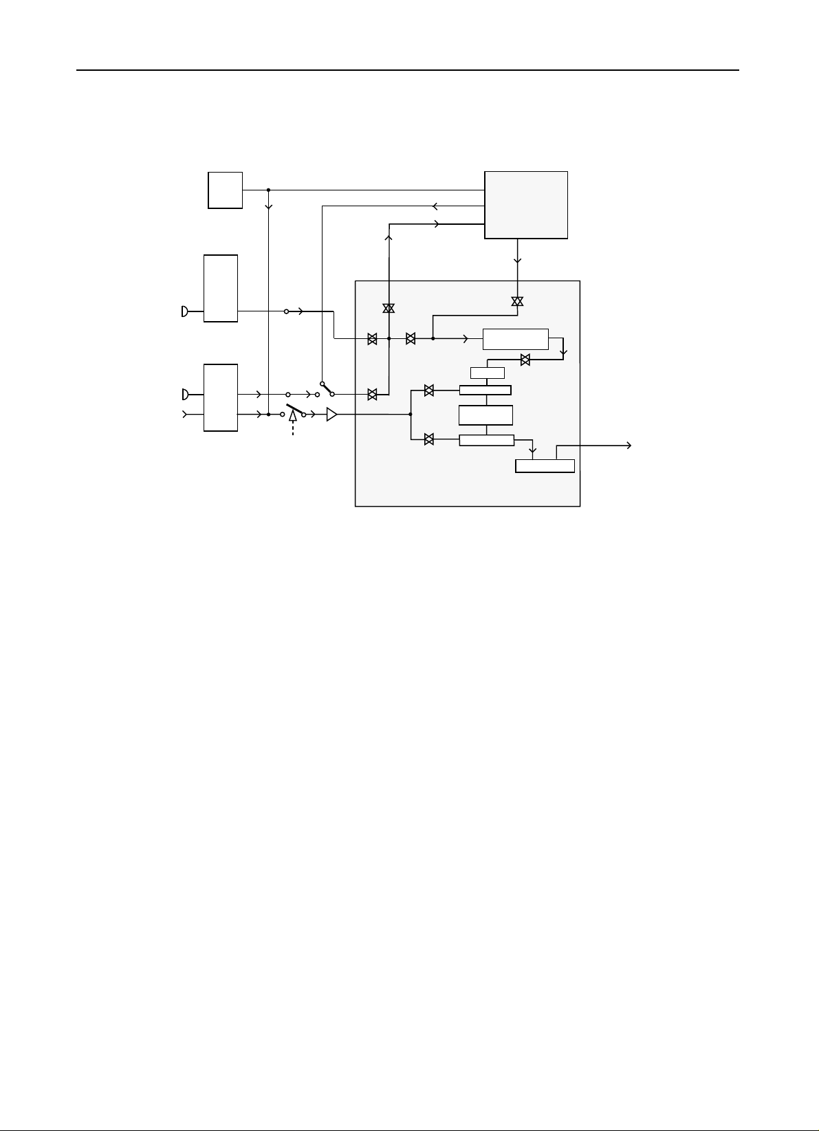
Refer to Figure 3-1 for reference for the following sections.
FLAT
TX RTN
MIC
EXT MIC
FLAT TX
AUDIO
J0451
18
EXPANSION BOARD
J0401
9
CONTROL HEAD
CONNECTOR
J0501
2
5
ACCESSORY
CONNECTOR
44
TX SND
TP0221
MIC
INT
46
MIC
ASFIC_CMP
IN
TP0222
FROM
µ
P Pin3
U0211-4
MIC
EXT
48
42
AUX
TX
Figure 3-1 Transmit Audio Paths
U0221
31
IN/OUT
39
OUT
33
IN
FILTERS AND
PREEMPHASIS
LIMITER
HS SUMMER
SPLATTER
FILTER
LS SUMMER
J0551
OPTION
BOARD
OUT
32
36
TX RTN
ATTENUATOR
VCO
ATN
40
MOD IN
TO
RF
SECTION
(SYNTHESIZER)
2.2.1 Mic/Data Input Path
The radio supports 2 distinct microphone paths known as internal (from controlhead) and external
mic (from accessory connector J0501-2) and an auxiliary path (FLAT TX AUDIO, from accessory
connector J0501-5). The microphones used for the radio require a DC biasing voltage provided by a
resistive network.
These two microphone audio input paths enter the ASFIC CMP at U0221-48 (external mic) and
U0221-46 (internal mic). Following the internal mic path; the microphone is plugged into the radio
controlhead and is connected to the controller board via J0401-9.
From here the signal is routed via R0409 and line INT MIC to R0205. R0201 and R0202 provide the
9.3VDC bias. Resistive divider R0205 / R0207 divide the input signal by 5.5 and provide input
protection for the CMOS amplifier input. R0202 and C0201 provide a 560 ohm AC path to ground
that sets the input impedance for the microphone and determines the gain based on the emitter
resistor in the microphone’s amplifier circuit.
C0204 serves as a DC blocking capacitor. The audio signal at U0221-46 (TP0221) should be
approximately 14mV for 1.5kHz or 3kHz of deviation with 12.5kHz or 25kHz channel spacing.
The external microphone signal enters the radio on accessory connector J0501 pin 2 and is routed
via line EXT MIC to R0206. R0203 and R0204 provide the 9.3VDC bias. Resistive divider R0206 /
R0208 divide the input signal by 5.5 and provide input protection for the CMOS amplifier input.
R0204 and C0202 provide a 560 ohm AC path to ground that sets the input impedance for the
microphone and determines the gain based on the emitter resistor in the microphone’s amplifier
circuit.
Page 15

Controller Board Audio and Signalling Circuits 1-11
C0254 serves as a DC blocking capacitor. Multi switch U0251 controlled by ASFIC CMP port GCB4
selects either the external microphone input signal or the voice storage playback signal for entering
the ASFIC CMP at pin 48. The audio signal at U0221-48 (TP0222) should be approximately 14mV
for 1.5kHz or 3kHz of deviation with 12.5kHz or 25kHz channel spacing.
The FLAT TX AUDIO path is used for transmitting data signals and has therefore no limiter or filters
enabled inside the ASFIC CMP. When this path is enabled via CPS and DATA PTT is asserted, any
signal on this path is directly fed to the modulator. Signals applied to this path either via accessory
connector J0501, expansion board connector J0451 or option board connector J0551 must be
filtered and set to the correct level externally or on the option board in order not to exceed the
maximum specified transmit deviation and transmitted power in the adjacent channels. The
attenuator inside the ASFIC CMP changes the FM deviation of the data signal according to the
channel spacing of the active transmit channel.
The FLAT TX AUDIO signal from accessory connector J0501-5 is fed to the ASFIC CMP (U0221)
pin42 through C0541 and line FLAT TX RTN, switch U0251 and buffer U0211-4. When the radio
switches from receive to transmit mode the µP opens switch U0251 for a short period to pre v ent that
any applied signal can cause a transmit frequency offset. Buffer U0211-4 sets the correct DC level
and ensures a short settle period when the radio is switched on. Inside the ASFIC CMP the signal is
routed directly to the attenuator, which sets the FM de viation according to the channel spacing of the
active transmit channel and emerges from the ASFIC CMP at U0221-40, at which point it is routed to
the RF section.
The ASFIC has an internal AGC that can control the gain in the mic audio path. The AGC can be
disabled / enabled by the µP. Another feature that can be enabled or disabled in the ASFIC is the
VO X. This circuit, along with the capacitor at U0221-7, provides a DC v oltage that can allow the µP to
detect microphone audio. The ASFIC can also be programmed to route the microphone audio to the
speaker for public address operation.
2.2.2 PTT Sensing and TX Audio Processing
Microphone PTT coming from the controlhead is sent via SBEP bus to the microprocessor. An
external PTT can be generated by grounding pin 3 on the accessory connector if this input is
programmed for PTT b y the CPS . When microphone PTT is sensed, the µP will always configure the
ASFIC CMP for the "internal" mic audio path, and external PTT will result in the external mic audio
path being selected.
Inside the ASFIC CMP, the mic audio is filtered to eliminate frequency components outside the 3003000Hz voice band, and pre-emphasized if pre-emphasis is enabled. The signal is then limited to
prevent the transmitter from over deviating. The limited mic audio is then routed through a summer,
which is used to add in signalling data, and then to a splatter filter to eliminate high frequency
spectral components that could be generated by the limiter. The audio is then routed to an
attenuator, which is tuned in the factory or the field to set the proper amount of FM deviation. The TX
audio emerges from the ASFIC CMP at U0221-40 MOD IN, at which point it is routed to the RF
section.
Dependent on the radio model, input pin 3 on the accessory connector can be programmed for D ATA
PTT by the CPS. When DATA PTT is sensed, the µP will always configure the ASFIC CMP for the flat
TX audio path. Limiter and an y filtering will be disabled. The signal is routed directly to the attenuator ,
which sets the FM deviation according to the channel spacing of the active transmit channel and
emerges from the ASFIC CMP at U0221-40, at which point it is routed to the RF section.
2.2.3 TX Secure Audio (optional)
The audio follows the normal transmit audio processing until it emerges from the ASFIC CMP TX
SND pin (U0221-44), which is fed to the Secure board residing at option connector J0551-33. The
Page 16
1-12 THEORY OF OPERATION
Secure board contains circuitry to amplify, encrypt, and filter the audio. The encrypted signal is then
fed back from J0551-32 to the ASFIC CMP TX RTN input (U0221-36). The signal level at this pin
should be about 65mVrms. The signal is then routed through the TX path in the ASFIC CMP and
emerges at MOD IN pin 40.
2.2.4 Option Board Transmit Audio
The audio follows the normal transmit audio processing until it emerges from the ASFIC CMP TX
SND pin (U0221-44), which is fed to the option board residing at option connector J0551-33. The
option board contains circuitry to process the audio. The processed signal is then fed back from
J0551-32 to the ASFIC CMP TX RTN input (U0221-36). The signal level at this pin should be about
65mVrms. The signal is then routed through the TX path in the ASFIC CMP and emerges at MOD IN
pin 40.
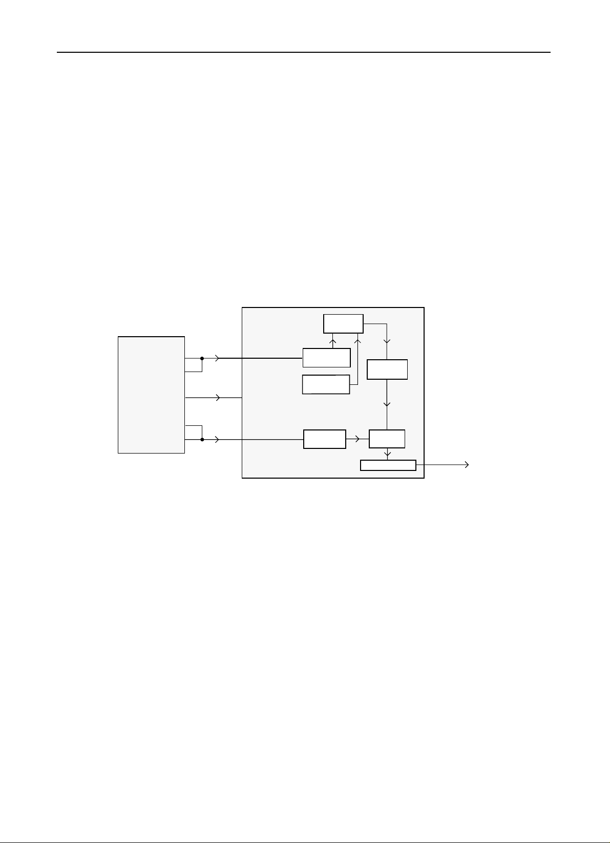
2.3 Transmit Signalling Circuits
Refer to Figure 4-1 for reference for the following sections.
HS
SUMMER
MICRO
CONTROLLER
U0101
44
82
SPI
BUS
85
80
HIGH SPEED
19
CLOCK IN
(HSIO)
LOW SPEED
18
CLOCK IN
(LSIO)
5-3-2 STATE
ENCODER
DTMF
ENCODER
ASFIC_CMP U0221
PL
ENCODER
SPLATTER
FILTER
LS
SUMMER
ATTENUATOR
40
MOD IN
TO RF
SECTION
(SYNTHESIZER)
Figure 4-1 Transmit Signalling Paths
From a hardware point of view, there are 3 types of signalling:
1) sub-audible data (PL / DPL / Connect Tone) that gets summed with transmit voice or signalling,
2) DTMF data for telephone communication in trunked and conventional systems, and
3) Audible signalling including Select 5, MPT-1327, MDC, High speed Trunking.
NOTE: All three types are supported by the hardware while the radio software determines which
signalling type is available.
2.3.1 Sub-audible Data (PL/DPL)
Sub-audible data implies signalling whose bandwidth is below 300Hz. PL and DPL waveforms are
used for conv entional operation and connect tones f or trunk ed v oice channel operation. The trunking
connect tone is simply a PL tone at a higher deviation level than PL in a conventional system.
Although it is referred to as "sub-audible data," the actual frequency spectrum of these waveforms
Page 17

Controller Board Audio and Signalling Circuits 1-13
may be as high as 250 Hz, which is audible to the human ear. However, the radio receiver filters out
any audio below 300Hz, so these tones are never heard in the actual system.
Only one type of sub-audible data can be generated by U0221 (ASFIC CMP) at any one time. The
process is as follows, using the SPI B US, the µP programs the ASFIC CMP to set up the proper lowspeed data deviation and select the PL or DPL filters. The µP then generates a square wave which
strobes the ASFIC PL / DPL encode input LSIO U0221-18 at twelve times the desired data rate. For
example, for a PL frequency of 103Hz, the frequency of the square wave would be 1236Hz.
This drives a tone generator inside U0221 which generates a staircase approximation to a PL sine
wave or DPL data pattern. This internal waveform is then low-pass filtered and summed with v oice or
data. The resulting summed waveform then appears on U0221-40 (MOD IN), where it is sent to the
RF board as previously described for transmit audio. A trunking connect tone would be generated in
the same manner as a PL tone.
2.3.2 High Speed Data
High speed data refers to the 3600 baud data waveforms, known as Inbound Signalling Words
(ISWs) used in a trunking system for high speed communication between the central controller and
the radio. To generate an ISW , the µP first prog r ams the ASFIC CMP (U0221) to the proper filter and
gain settings. It then begins strobing U0221-19 (HSIO) with a pulse when the data is supposed to
change states. U0221’s 5-3-2 State Encoder (which is in a 2-state mode) is then fed to the postlimiter summer block and then the splatter filter. From that point it is routed through the modulation
attenuators and then out of the ASFIC CMP to the RF board. MPT 1327 and MDC are generated in
much the same way as Trunking ISW. However, in some cases these signals may also pass through
a data pre-emphasis block in the ASFIC CMP. Also these signalling schemes are based on sending
a combination of 1200 Hz and 1800 Hz tones only. Microphone audio is muted during High Speed
Data signalling.
2.3.3 Dual Tone Multiple Frequency (DTMF) Data
DTMF data is a dual tone waveform used during phone interconnect operation. It is the same type of
tones which are heard when using a "Touch Tone" telephone.
There are seven frequencies , with four in the low group (697, 770, 852, 941Hz) and three in the high
group (1209, 1336, 1477Hz).
The high-group tone is generated by the µP (U0101-44) strobing U0221-19 at six times the tone
frequency for tones less than 1440Hz or twice the frequency for tones g reater than 1440Hz. The low
group tone is generated by the ASFIC CMP, controlled by the µP via SPI bus. Inside U0221 the lowgroup and high-group tones are summed (with the amplitude of the high group tone being
approximately 2 dB greater than that of the low group tone) and then pre-emphasized before being
routed to the summer and splatter filter. The DTMF waveform then follows the same path as was
described for high-speed data.
Page 18
1-14 THEORY OF OPERATION
2.4 Receive Audio Circuits
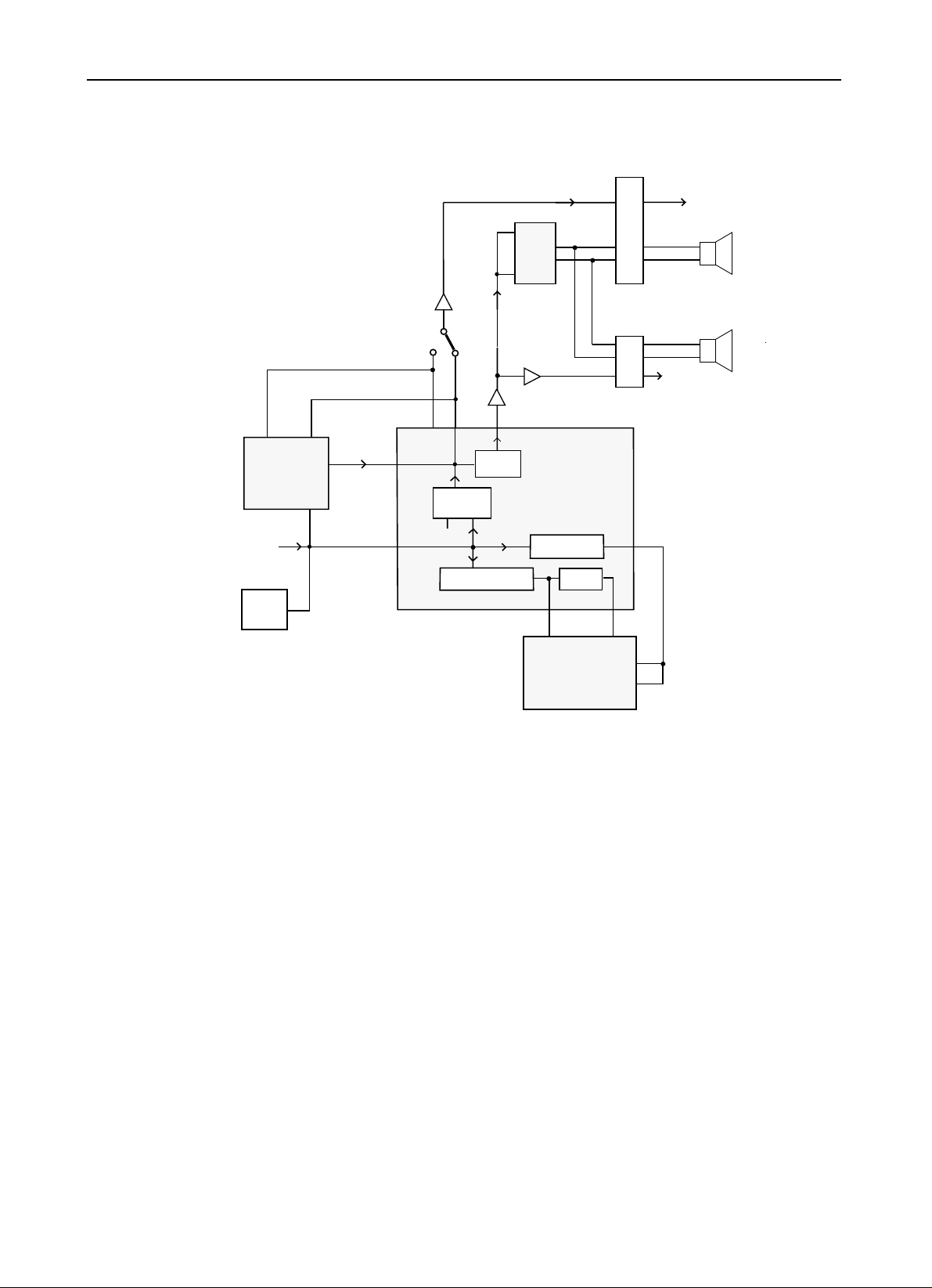
Refer to Figure5-5 for reference for the following sections.
ACCESSORY
CONNECTOR
11
FLT/FLAT RX AUDIO
SPKR +
SPKR -
INT
SPKR-
CONTROLHEAD
CONNECTOR
LS IO
SQ DET
17
83
J0501
J0401
18
80
85
16
1
3
2
7
HANDSET
AUDIO
EXTERNAL
SPEAKER
INTERNAL
SPEAKER
35
IN
OPTION
BOARD
J0551
FROM
RF
SECTION
(IF IC)
J0451
EXPANSION
BOARD
DISC
AUDIO
17
OUT
IN
7
1
AUDIO
4
PA
U0271
9
39
28
IN
34
43
U IO
AUX RX
URX OUT
4110
AUDIO
VOLUME
ATTEN.
6
INT
SPKR+
ASFIC_CMP
U0221
FILTER AND
DEEMPHASIS
DISC
2
LIMITER, RECTIFIER
FILTER, COMPARATOR
CH ACT
PL FILTER
LIMITER
SQUELCH
CIRCUIT
16
84
MICRO
CONTROLLER
U0101
2.4.1 Squelch Detect
The radio’s RF circuits are constantly producing an output at the discriminator (IF IC). This signal
(DISC AUDIO) is routed to the ASFIC CMP’s squelch detect circuitry input DISC (U0221-2). All of
the squelch detect circuitry is contained within the ASFIC CMP. Therefore from a user’s point of vie w,
DISC AUDIO enters the ASFIC CMP, and the ASFIC CMP produces two CMOS logic outputs based
on the result. They are CH ACT (U0221-16) and SQ DET (U0221-17).
The squelch signal entering the ASFIC CMP is amplified, filtered, attenuated, and rectified. It is then
sent to a comparator to produce an active high signal on CH ACT. A squelch tail circuit is used to
produce SQ DET (U0221-17) from CH ACT. The state of CH ACT and SQ DET is high (logic 1) when
carrier is detected, otherwise low (logic 0).
CH ACT is routed to the µP pin 84 while SQ DET is routed to the µP pin 83.
SQ DET is used to determine all audio mute / unmute decisions except for Conventional Scan. In
this case CH ACT is a pre-indicator as it occurs slightly faster than SQ DET.
Figure 4-1 Receive Audio Paths
Page 19

Controller Board Audio and Signalling Circuits 1-15
2.4.2 Audio Processing and Digital Volume Control
The receiver audio signal enters the controller section from the IF IC on DISC AUDIO. The signal is
DC coupled by R0228 and enters the ASFIC CMP via the DISC pin U0221-2.
Inside the ASFIC CMP, the signal goes through 2 paths in parallel, the audio path and the PL/DPL
path.
The audio path has a programmable amplifier, whose setting is based on the channel bandwidth
being received, then a LPF filter to remove any frequency components above 3000Hz and then an
HPF to strip off any sub-audible data below 300Hz. Next, the recovered audio passes through a deemphasis filter if it is enabled (to compensate for Pre-emphasis which is used to reduce the eff ects of
FM noise). The IC then passes the audio through the 8-bit programmable attenuator whose level is
set depending on the value of the volume control. Finally the filtered audio signal passes through an
output buffer within the ASFIC CMP. The audio signal exits the ASFIC CMP at pin AUDIO (U0221-
41).
The µP programs the attenuator, using the SPI BUS, based on the volume setting. The minimum /
maximum settings of the attenuator are set by codeplug parameters.
Since sub-audible signalling is summed with voice inf ormation on transmit, it must be separated from
the voice information before processing. Any sub-audible signalling enters the ASFIC CMP from the
IF IC at DISC U0221-2. Once inside it goes through the PL/DPL path. The signal first passes through
one of 2 low pass filters, either PL low pass filter or DPL/LST low pass filter. Either signal is then
filtered and goes through a limiter and exits the ASFIC CMP at LSIO (U0221-18). At this point the
signal will appear as a square wave version of the sub-audible signal which the radio received. The
microprocessor U0101-80 will decode the signal directly to determine if it is the tone / code which is
currently active on that mode.
2.4.3 Audio Amplification Speaker (+) Speaker (-)
The output of the ASFIC CMP’s digital v olume pot, U0221-41 is routed through dc b loc king capacitor
C0265 to a buffer formed by U0211-1. Resistors R0265 and R0268 set the correct input level to the
audio PA (U0271). This is necessary because the gain of the audio PA is 46 dB, and the ASFIC CMP
output is capable of overdriving the PA unless the maximum volume is limited. Resistor R0267 and
capacitor C0267 increase frequency components below 350 Hz.
The audio then passes through R0269 and C0272 which provides AC coupling and low frequency
roll-off. C0273 provides high frequency roll-off as the audio signal is routed to pins 1 and 9 of the
audio power amplifier U0271.
The audio power amplifier has one inverted and one non-inverted output that produces the
differential audio output SPK+ / SPK- (U0271-4/6). The inputs for each of these amplifiers are pins 1
and 9 respectively; these inputs are both tied to the received audio. The audio PA’s DC biases are
not activated until the audio PA is enabled at pin 8.
The audio PA is enabled via the ASFIC CMP (U0221-38). When the base of Q0271 is low, the
transistor is off and U0271-8 is high, using pull up resistor R0273, and the Audio PA is ON. The
voltage at U0273-8 must be above 8.5VDC to properly enable the device. If the voltage is between
3.3 and 6.4V, the device will be active but has its input (U0273-1/9) off . This is a mute condition which
is used to prevent an audio pop when the PA is enabled.
The SPK+ and SPK- outputs of the audio PA have a DC bias which varies proportionately with FLT
A+ (U0271-7). FLT A+ of 11V yields a DC offset of 5V, and FLT A+ of 17V yields a DC offset of 8.5V .
If either of these lines is shorted to ground, it is possible that the audio PA will be damaged. SPK+
and SPK- are routed to the accessory connector (J0501-16 and 1) and to the controlhead (connector
J0401-2 and 3).
Page 20

1-16 THEORY OF OPERATION
2.4.4 Handset Audio
Certain hand held accessories have a speaker within them which require a different voltage level
than that provided by U0271. For those devices HANDSET AUDIO is available at controlhead
connector J0401-7.
The received audio from the output of the ASFIC CMP’s digital volume attenuator and buffered by
U0211-1 is also routed to U0211-3 pin 9 where it is amplified 20 dB; this is set by the 10k/100k
combination of R0261 and R0262. This signal is routed from the output of the op amp U0211-3 pin 8
to J0401-7. The controlhead sends this signal directly out to the microphone jack. The maximum
value of this output is 6.6Vp-p.
2.4.5 Filtered Audio and Flat Audio
The ASFIC CMP has an audio whose output at U0221-39 has been filtered and de-emphasized, but
has not gone through the digital volume attenuator. From ASFIC CMP U0221-39 the signal is routed
via R0251 through gate U0251-12 and AC coupled to U0211-2. The gate controlled by ASFIC CMP
port GCB3 (U0221-35) selects between the filtered audio signal from the ASFIC CMP pin 39
(URXOUT) or the unfiltered (flat) audio signal from the ASFIC CMP pin 10 (UIO). R0251 and R0253
determine the gain of op-amp U0211-2 for the filtered audio while R0252 and R0253 determine the
gain for the flat Audio. The output of U0253-7 is then routed to J0501-11 via dc blocking capacitor
C0542 and R0531. Note that any volume adjustment of the signal on this path must be done by the
accessory
2.4.6 RX Secure Audio (optional)
Discriminator audio, which is now encrypted audio, f ollo ws the normal receive audio processing until
it emerges from the ASFIC CMP UIO pin (U0221-10), which is fed to the Secure board residing at
option connector J0551-35. On the Secure board, the encrypted signal is converted back to normal
audio format, and then fed back through (J0551-34) to AUX RX of the ASFIC CMP (U0221-43).
From then on it follows a path identical to conventional receive audio, where it is filtered (0.3 - 3kHz)
and de-emphasized. The signal URX SND from the ASFIC CMP (U0221-39), also routed to option
connector J0551-28, is not used for the Secure board but for other option boards.
2.4.7 Option Board Receive Audio
Unfiltered audio from the ASFIC CMP pin UIO (U0221-10) enters the option board at connector
J0551-35. Filtered audio from the ASFIC CMP pin URXOUT (U0221-39) enters the option board at
connector J0551-28. On the option board, the signal may be processed, and then fed back through
J0551-34 to AUX RX of the ASFIC CMP (U0221-43). From then on it follows a path identical to
conventional receive audio, where it may be filtered (0.3 - 3kHz) and de-emphasized.
Page 21
Controller Board Audio and Signalling Circuits 1-17
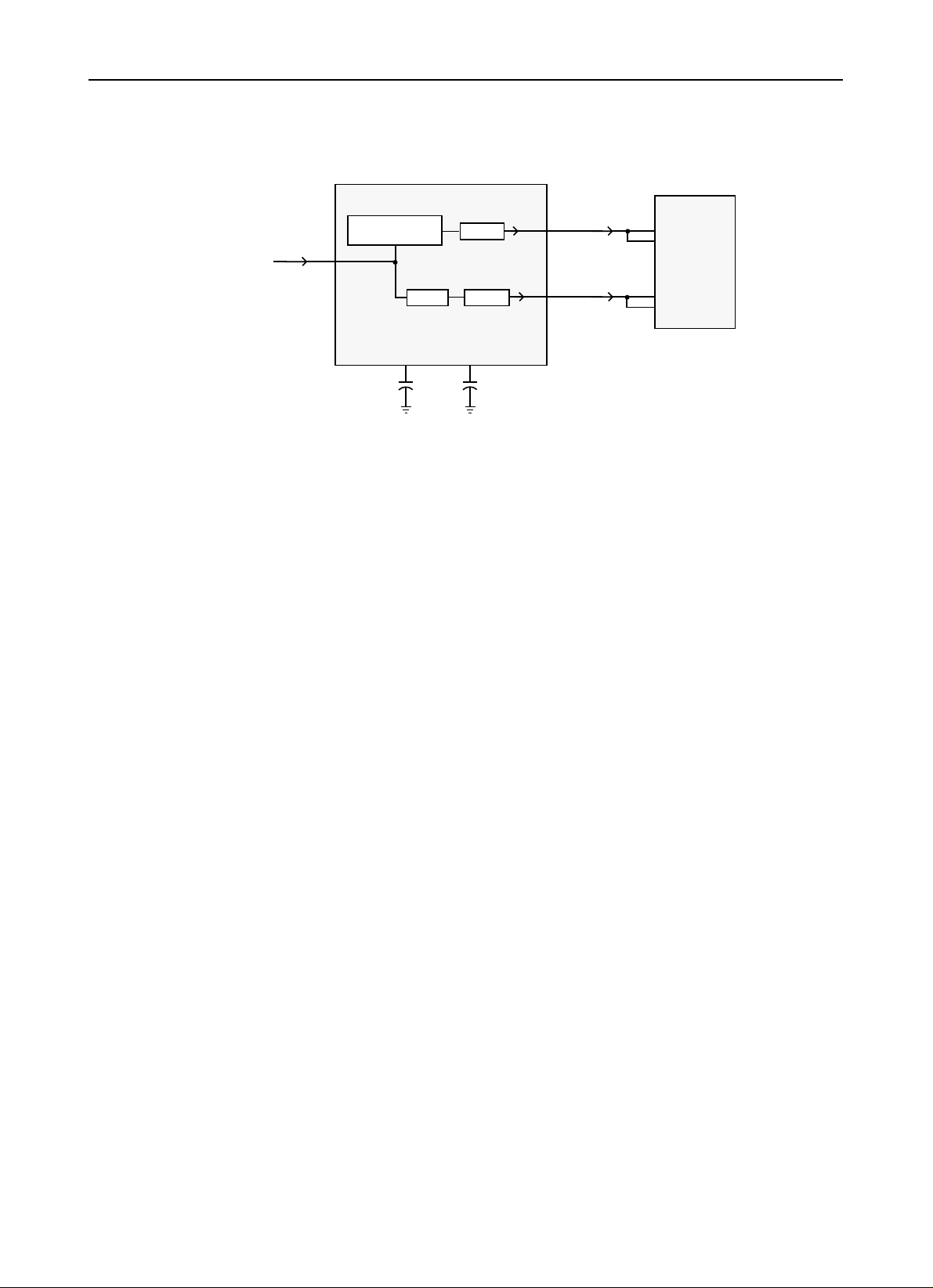
2.5 RECEIVE SIGNALLING CIRCUITS
Refer to Figure 5-6 for reference for the following sections.
DET AUDIO
DISCRIMINATOR AUDIO
FROM RF SECTION
(IF IC)
AND DEEMPHASIS
DISC
2
DATA FILTER
FILTER
PLCAP
8
LIMITER
ASFIC_CMP
U0221
LIMITER
PLCAP2
HSIO
LSIO
25
Figure 4-2 Receive Signalling Paths
2.5.1 Sub-audible (PL/DPL) and High Speed Data Decoder
The ASFIC CMP (U0221) is used to filter and limit all received data. The data enters the ASFIC CMP
at input DISC (U0221-2). Inside U0221 the data is filtered according to data type (HS or LS), then it
is limited to a 0-5V digital level. The MDC and trunking high speed data appear at U0221-19, where
it connects to the µP U0101-82
The low speed limited data output (PL, DPL, and trunking LS) appears at U0221-18, where it
connects to the µP U0101-80.
The low speed data is read by the µP at twice the frequency of the sampling waveform; a latch
configuration in the ASFIC CMP stores one bit every clock cycle . The external capacitors C0236, and
C0244 set the low frequency pole for a zero crossings detector in the limiters for PL and HS data.
The hysterisis of these limiters is programmed based on the type of received data.
19
18
82
CONTROLLER
44
80
85
MICRO
U0101
2.5.2 Alert Tone Circuits
When the software determines that it needs to give the operator an audible f eedbac k (for a good key
press, or for a bad key press), or radio status (trunked system busy, phone call, circuit failures), it
sends an alert tone to the speaker. It does so by sending SPI BUS data to U0221 which sets up the
audio path to the speaker for alert tones. The alert tone itself can be generated in one of two ways:
internally by the ASFIC CMP, or externally using the µP and the ASFIC CMP.
The allowable internal alert tones are 304, 608, 911, and 1823Hz. In this case a code contained
within the SPI BUS load to the ASFIC CMP sets up the path and determines the tone frequency , and
at what volume lev el to gener ate the tone. (It does not have to be related to the voice v olume setting).
For external alert tones, the µP can generate any tone within the 100-3000Hz audio band. This is
accomplished by the µP generating a square wave which enters the ASFIC CMP at U0221-19.
Inside the ASFIC CMP this signal is routed to the alert tone generator
The output of the generator is summed into the audio chain just after the RX audio de-emphasis
block. Inside U0221 the tone is amplified and filtered, then passed through the 8-bit digital volume
attenuator, which is typically loaded with a special v alue for alert tone audio. The tone exits at U022141 and is routed to the audio PA like receive audio
Page 22

1-18 THEORY OF OPERATION
2.6 Voice Storage (optional)
The Voice Storage (VS) option can be used to store audio signals coming from the receiver or from
the microphone. Any stored audio signal can be played back over the radio’s speaker or sent out via
the radio’s transmitter.
The Voice Storage option can by placed on the controller section or on an additional option board
which resides on option board connector J0551. Voice Storage IC U0301 provides all required
functionality and is powered from 3.3 volts regulator U0351 which is powered from the regulated 5
volts. Dual shottky diode D0301 reduces the supply voltage for U0301 to 3 volts. The microprocessor
controls U0301 via SPI bus lines CLK (U0301-8), DATA (U0301-10) and MISO (U0301-11). To
transfer data, the µP first selects the U0301 via address decoder U0141, line VS CS and U0301 pin
9. Then the µP sends data through line DATA and receives data through line MISO. Pin 2 (RAC) of
U0301 indicates the end of a message row by a low state for 12.5 ms and connects to µP pin 52. A
low at pin 5 (INT), which is connected to µP pin 55 indicates that the Voice Storage IC requires
service from the µP.
Audio, either from the radio’s receiver or from one of the microphone inputs, emerges the ASFIC
CMP (U0221) at pin 39, is buffered by op-amp U0341-1 and enters the Voice Storage IC U0301 at
pin 25. During pla yback, the stored audio emerges U0301 at pin 20. To transmit the audio signal it is
fed through resistive divider R0344 / R0345 and line VS MIC to input selector IC U0251. When this
path is selected by the µP via ASFIC CMP port GCB 4, the audio signal enters the ASFIC CMP at
pin 48 and is processed like normal transmit audio. To play the stored audio over the r adio’ s speak er,
the audio from U0301 pin 20 is buffered b y op-amp U0341-2 and f ed via s witch U0342 and line FLAT
RX SND to ASFIC CMP pin 10 (UIO). In this case , this ASFIC CMP pin is programmed as input and
feeds the audio signal through the normal receiver audio path to the speaker or handset. Switch
U0342 is controlled by the µP via ASFIC CMP port GCB 4 and feeds the stored audio only to the
ASFIC CMP port UIO when it is programmed as input.
Page 23
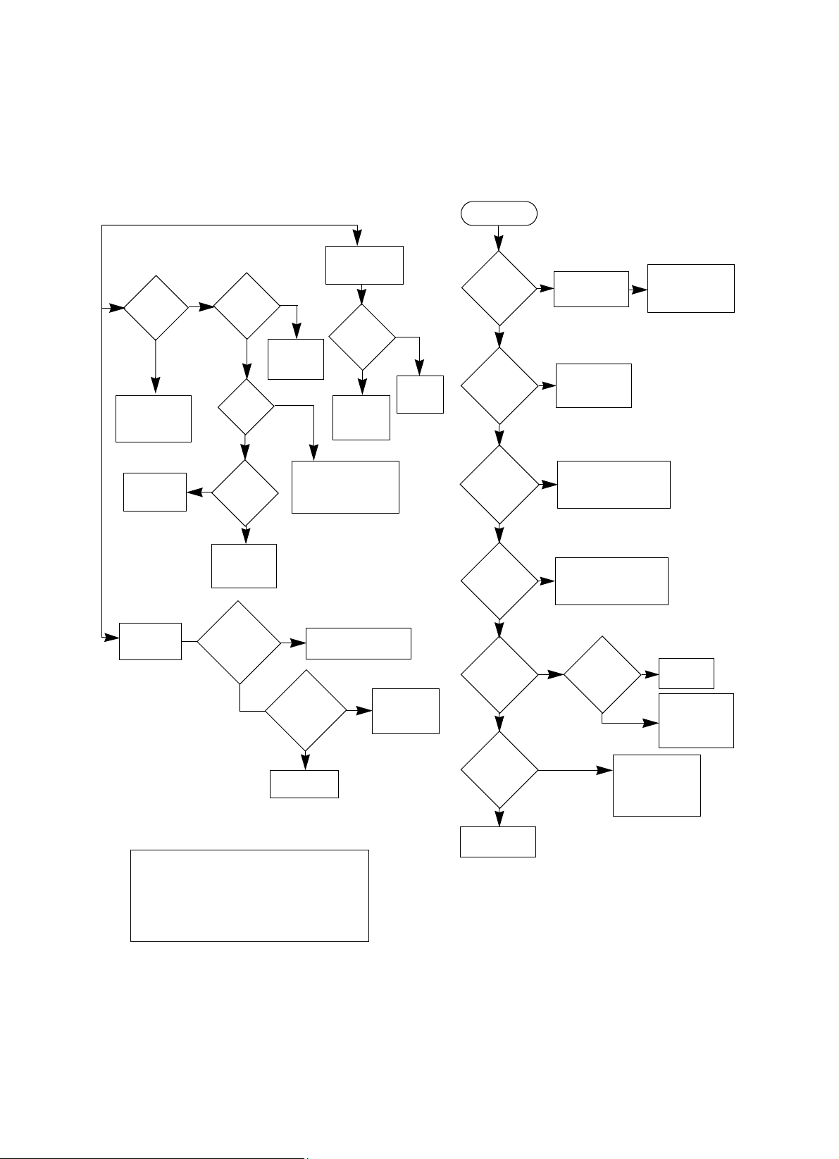
TROUBLESHOOTING CHARTS
1.0 Controller T roubleshooting Chart
Chapter 2
RX
AUDIO
Audio at Pin
Check Spk.
Flex Connection & Control
Check Re-
EXT
PTT
Radio could
not PTT
externally
J0501
16 &
Pin 1
YES
ceiver &
IF IC
NO
Audio
at Audio PA
(U0271)
input
NO
Audio
at Pin 41
U0221?
NO
Audio at
Pin 2
U0221?
Check ASFIC U0221
External PTT enabled with CPS?
YES
NO
YES
YES
Check
Audio PA
(U0271)
YES
Check Components
between U0221 and
NO
Enable External PTT
DC
at as-
signed Acc.
Con. Pin
DC chang-
es?
NO
Check
Accessories
PTT
Press PTT. No
RF Output Pow-
er.
Red LED
lights up?
YES
Check
FGU &
Transmitter
U0271
with CPS
Check Con-
YES
nection to uP
NO
Check
Control
Head
port
Controller Check
Power Up
Alert Tone
OK?
NO
Speaker &
Control
Head OK?
YES
9.3V
DC at Pin 5
of U0641?
YES
5V DC at
Pin OUT of
U0651?
YES
U0101
EXTAL=
7.3728 MHz/
14.7456
MHz?
YES
BUS+
activity when
volume knob
rotated?
YES
Not able to
YES
program
RF Board ICs
Replace
NO
Speaker / Con-
trol Head
NO
Check U0641, Q0641,
Q0661, D0660 &
NO
Check U0651, D0651,
NO
U0221 Pin 34 =
16.8 MHz?
NO
D0661
D0621
YES
Head and MCU
(U0101, U0121,
U0122, U0111)
Before replacing
MCU, check SPI
clock, SPI data,
and RF IC select
NO
Check
FGU
Reprogram the
correct data. &
Check ASFIC
and MCU
Check Control
Before troubleshooting the controller section according to this chart please check the following:
1. Check tuning and CPS settings
2. Check if Alert Tones are enabled
3. Check if Control Head is OK
4. Check board visually
MCU is OK
Page 24

2-2 TROUBLESHOOTING CHARTS
Page 25

CONTROLLER SCHEMATICS / PARTS LIST
1.0 Allocation of Schematics and Circuit Boards
1.1 Controller Circuits
This Chapter shows the Schematics and the the Parts Lists for the Controller circuits.
1.2 Voice Storage Facility
The Voice Storage is fitted on all MPT radios GM640/660/1280 and on GM380 as standard.
The schematics, component layout and parts list for these circuits are shown in this chapter.
The Voice Storage schematic is shown in Tables below.
Table 3-1 Controller T2 Diagrams and Parts Lists
Controller T2 used on PCB :
8486172B04 VHF, 1-25W
SCHEMATICS
Controller Overall
Supply V oltage
Audio
I/O
Microprocessor
Parts List
Controller T2 Page 3-8
Page 3-3
Page 3-4
Page 3-5
Page 3-6
Page 3-7
Chapter 3
.
Table 3-2 Controller T5 Diagrams and Parts Lists
Controller T5 used on PCB :
8486172B06 VHF, 1-25W
SCHEMATICS
Controller Overall
Supply V oltage
Audio
I/O
Microprocessor
Voice Storage (if fitted)
Parts List
Controller T5 Page 3-16
Page 3-10
Page 3-11
Page 3-12
Page 3-13
Page 3-14
Page 3-15
Page 26

3-2 Controller schematics / parts list
.
Table 3-3 Controller T6 Diagrams and Parts Lists
Controller T6/T7 used on PCB :
T6 on 8486206B06 LB1, 60W
T6 on 8486140B12 VHF, 25-45W
T6 on 8480643z06 UHF B1, 25-40W
T7 on 8486172B07 VHF, 1-25W
T7 on 8485670z02 UHF B1, 1-25W
SCHEMATICS
Controller Overall
Supply V oltage
Audio
I/O T6
I/O T7
Microprocessor
Voice Storage (if fitted)
Page 3-19
Page 3-20
Page 3-21
Page 3-22
Page 3-23
Page 3-24
Page 3-25
Parts List
Controller T6/T7 Page 3-26
 Loading...